2008년 9월 29일 월요일

How to defend against the cloning of your FPGA designs | Programmable Logic DesignLine


September 17, 2008
 
How to defend against the cloning of your FPGA designs
 
Having your design cloned by a competitor isn't fun, so this "How To" design article explains how to foil your nefarious foes!
 
Editor's Note: The technique described in this article is actually rather clever. May I suggest that, after reading the first section, you pause for a moment and try to guess how the DesignTag concept described below might be implemented. I bet that when you move on to the "So how does it work?" section you'll say to yourself (as I did): "Wow, I would never have thought of that!"


This article describes a new way of tagging designs to help to counter the rapidly growing trade in stolen IP and cloned designs. The topic is a difficult one for the industry to discuss; recently, however, more and more voices have been raised on the issue.

An estimate of the prevalence of counterfeit electronics has been put as high as 10%. (The International Chamber of Commerce website, for example, includes the statement: "Counterfeit electronics are estimated to account for 1 to 10 % of global electronic sales"). This is supported by the Alliance for Gray Markets and Counterfeit Abatement (AGMA) (www.agmaglobal.org), an industry group that consists of Hewlett Packard, Cisco, and other top tier electronics OEM companies, which estimates the loss to manufacturers at more than $100B. The hidden costs of damaged reputations and reliability issues for the end customer are more difficult to quantify.

One unfortunate consequence of the rise of programmable logic coupled with the decline of the ASIC is that it is now easier than ever to copy a design. Some Asian or Eastern European companies openly claim to specialise in "reverse engineering" or copying PCB layouts and memory contents. It is difficult, expensive, and time consuming to reverse engineer an ASIC, but simple to copy the configuration bit stream of the most popular FPGAs (see *note) as illustrated in Fig 1.


1. Stealing an FPGA design is not complex.

*Note: It is possible to encrypt bit streams for some SRAM based FPGAs. However, the overwhelming majority of customers do not use this because of added cost, complexity and logistics. The feature is not offered in the low cost parts that most customers use for high volume applications. Non-volatile FPGAs avoid this, but comprise only a small fraction of the overall market.

As a result, companies can find that overnight their Intellectual Property (IP) appears in the product of a competitor. The counterfeiter carries virtually no R&D cost, and can therefore undercut the legitimate supplier on price and steal market share.

The problem is how to deter theft and prove ownership of the design. This is where a product called DesignTag from Algotronix can help. When buried in the FPGA bit-stream, the DesignTag code is very difficult to locate and disable – even if the fraudster knows that it is included.

Once this code is duplicated into the pirated bit-stream, it acts like a beacon announcing that the design has been copied. There is a strong parallel with the concept of marking valuables with your Post Code or Zip code using UV pens. It cannot prevent the theft, but allows ownership to be established afterwards.


2. DesignTag provides "proof-of-theft".

The DesignTag occupies $0.57 cents worth of silicon in a XC3S2000 FPGA (using the 100+ list pricing), which represents 1.3% of the logic resources on the chip. This is a modest overhead compared to the potential damage represented by illegal copies.

A more insidious problem comes from so called "over-building". The background to this problem lies in the mass exodus over the last decade of companies exiting production in favour of designing products to be built by contract manufacturers (CEM). This positions the CEM in a central and critical role. The vast majority of CEMs, of course, are responsible and provide a valuable service. Unscrupulous ones, however, can supplement their profits by producing more units than they are contracted for and selling the excess onto the gray market. Again the DesignTag identifies the source and ownership of the design.

A further application of DesignTag is to provide serial numbering or version identification. For example, medical, automotive, industrial, military, or aerospace manufacturers may wish to tag equipment with end customer codes or track the FPGA configuration version. Version control is especially important where upgrades are routinely applied. The DesignTag can be detected in working systems without making electrical contact and is particularly beneficial for ball grid arrays where the top of the package is far more accessible than the electrical connections. Monitoring can also be achieved without resorting to software or hardware interrupts that might affect the normal operation.

Yet another twist is to have an embedded system interact with DesignTag so that it flags fault or status conditions. In this application, the DesignTag is programmed to output a different code that unobtrusively signals the internal condition.

So how does it work?
This is really going to surprise you... go to page 2 of this article for all to be revealed...

So how does it work?
DesignTag is a small low-cost IP core that can be included into an FPGA as part of the design. It is a digital core with a unique code ("signature") that can be identified externally without needing to read the FPGA bit stream or internal registers.

It works by modulating the power dissipation of the host device in a predefined way. Tiny heat pulses propagate through the chip package with low attenuation. The level of the power "surge" is selected to provide a package temperature rise of only about 0.1 degrees C. The additional dissipation is typically 5mW, against an operational power consumption of >150mW for a mid-sized Spartan FPGA, which means the signal is deep below the noise floor.

The DesignTag defaults to turn off after 15 minutes of operation (the user can modify this value). This has two effects. Firstly it eliminates the small incremental power consumption, and secondly it also makes detection by a fraudster more difficult as power has to be cycled. Optionally, DesignTag can be triggered by an internal event from within the FPGA. This could be an instruction to transmit the ID code or to indicate an internal status or error condition.

The DesignTag database
The code data for all DesignTags is held in a central data base. Customers can choose whether they wish to make their code "public" or "private". The advantage of a public listing is that all DesignTag Reader
Software will be enabled to detect the code, thereby allowing customers, enforcement agencies, and contract manufacturers to confirm the validity of the device under test (DUT).

By comparison, private codes may be preferred when the customer does not wish any third-parties to be able to tell whether or not their product is tagged. In this case codes are distributed by the customer to trusted parties – only their reader software with these codes installed will be enabled to detect the corresponding tags.

Incorporating DesignTag into an FPGA
The IP core for use with FPGAs is instantiated into HDL code as a "black box" in either Verilog or VHDL. The deliverable includes the in-built code which will drive the thermal output, as well as
I/O pins that are required by the circuit. The all-digital design has a small footprint, typically requiring only 256 slices in a Spartan 3 FPGA from Xilinx.

The core is only available as an encrypted EDIF netlist for security reasons. The IP includes several techniques to prevent "reverse engineering" as well as other schemes designed to mask it from being tampered with or detected.

The core is largely independent of the user design, so the impact on the design flow is minimal.

DesignTag takes an input clock in the range 2-to-250MHz to drive the timing. The clock should be derived from any available clock inside the system rather than being generated specifically for the tag IP core for two reasons. Primarily, of course, it is the lowest cost option, but also it confuses attempts to detect and disable the tag by making it appear to merge into the system.

Control inputs for the DesignTag can be driven from the embedded system or set as defaults at the design stage. For example, the core can be set to transmit continuously if required; alternatively, the core can be instructed to transmit for a specified time on power-up, and to then enter a stand-by mode. As yet another option, the transmit sequence can be initiated at any time by a Trigger input.

The core is licensed with up to four different in-built codes, which are selected by the Code Select inputs. The embedded system can program the core to transmit one of these codes on command to indicate internal status conditions. For example, conditions indicating that an overflow has occurred or a soft error was detected in memory can be signalled without interrupting the system functionality.

A Tamper Output can be taken from the DesignTag into the embedded system. This has two benefits. It can be used as a disable signal that impairs the system performance and confuses an attempt to disable the tag by flipping random bits in the configuration bit stream. The second benefit is that if an attacker reverse engineers the bit stream to reconstitute the design, then the DesignTag block will appear as an integral part of the design.

Detecting DesignTag outputs
DesignTag codes are detected by placing a thermocouple in good thermal contact with the top of the package while the device is in operation as illustrated in Fig 3.


3. Detecting thermal signals with a thermocouple.

The thermal readings are input into the DesignTag Reader Software, which decrypts the signals. Detection time for a positive recognition of a code is measured in minutes, and the system can detect and differentiate multiple tags within the same device.

Poor conditions may increase the time required, but the underlying algorithms accumulate confidence with increased sample sizes (Fig 4). Acquisition time can be reduced if readings are taken in still air. The self-heating of the DUT as power is applied will not prevent the tag being detected. Factors that could increase the detection time include thermally erratic conditions, poor contact between the probe and the package or multiple codes in a single design.


4. The signals are accumulated and processed until a high confidence is achieved.
(Click this image to view a larger, more detailed version)

The DesignTag works with all popular styles of packages. However DesignTag is not recommended, at this time, for use with heatsinks or where forced air cooling is employed.

Algotronix recommends the TC-08 data logger with thermocouple from Pico Technology. Further devices are being evaluated. A TC-08 is included as part of the DesignTag Starter Kit along with the Reader Software, an evaluation board equipped with an FPGA and five active DesignTag codes (Fig 5). The Reader Software runs on a PC under Windows (XP or Vista).


5. The Starter Kit includes the Data Logger, Software, Evaluation Board, and five unique codes.
(Click this image to view a larger, more detailed version)

Attempting to defeat DesignTag
One of the most important features for any anti-counterfeiting scheme is the difficulty of identifying, removing, or disabling the identity tag. This article will not go into a detailed description of the in-built countermeasures against removal and reverse engineering for obvious reasons, but let's consider how a counterfeiter might approach the job of defeating DesignTag.

The first problem for a potential thief is to identify if the stolen code contains the DesignTag or not. The tiny thermal signals take the form of a 64-bit code and can only be detected by using DSP and decryption techniques. A spreading code is used to control the heat generator using a Linear Feedback Shift Register (LFSR) like circuit (see *note).

*Note: See also this Three-part mini-series on LFSRs.

The spreading code generation circuit is based on the unique 'Tag ID', which acts like a cryptographic key, where each key results in a different pseudo-noise sequence. The DesignTag Reader Software will readily identify public codes, but without prior knowledge and authorisation, the software is not enabled to detect private codes, which will remain hidden.

Various aspects of the tag waveform are pseudo-random. The code is designed to frustrate attempts to decode the signals by repeated power cycling and correlating the observed signals.

Another possible attack is to obtain multiple DesignTag IP cores and compare them at the bit-stream or encrypted netlist level in order to see which specific resources have changed on the assumption that these will correspond to code bits. To frustrate this attack, many aspects of the tag IP core are varied in a random manner to create a very large numbers of differences between any two tag instances.

An attacker may try to disable the DesignTag. It is instantiated into an FPGA design as a black box at the design capture stage and once included is incorporated into the bit stream that configures the SRAM device. Users can choose to encrypt their bit stream, but most do not.

FPGA configuration bit streams typically range from 2 Mb for a mid-range Spartan device, through to 10's of Mb for the larger Virtex family. Fraudsters may attempt to use software to reconstruct a netlist from the bit-stream information.

While such software has been created in the past and has been reported in the technical literature it appears that such tools are not currently openly available to hackers. The output of such software would be a flat netlist of the design after mapping onto FPGA primitives; while this is a step forward from a bit-stream, it is still a long way from the original design source code.

The fraudster could also try and manipulate the design at the bit-stream level by selectively 'flipping' bits and monitoring the effect with a view to shutting off security features. This is a more practical attack since it does not depend on developing or acquiring bit-stream reverse engineering software. It does require recalculating the checksum on the FPGA bit-stream so it is not totally straightforward.

The key to defeating this attack is to make the time needed for each 'flip a bit and see what happens' cycle as long as possible and to make it difficult for an attacker to determine whether the security features have in fact been completely disabled. The fact that it takes several minutes to read a DesignTag code makes search based attacks such as this less feasible.

An advantage of DesignTag compared with FPGA design security mechanisms such as Device DNA or challenge/response schemes which involve accessing an external chip through I/O pins is that DesignTag is not tied to specific resources on the FPGA which have easily determined locations in the bitstream.

FPGAs based on Flash or anti-fuse technology are configured in the factory and so the code containing the DesignTag is not exposed to the end user. Any attack on the DesignTag would involve physically tampering with the device and result in destroying the FPGA.

Why thermal and not electrical signals?
By this time you are probably wondering why an unconventional signalling medium was chosen.

The most obvious mechanism to signal to circuits within a chip is through package pins. However, there are important drawbacks to this mechanism in this context. To be useful to an end user, the tag mechanism has to be independent of the circuit board onto which the chip has been designed and independent of any system software.

In some cases, the developer of the circuit board and system software may be the party suspected of misuse of the IP. Also, accessing the tag should not require detailed knowledge of the system containing the suspect chip. With BGA chips and fine pitch flat packs, even the act of finding an appropriate place on a circuit board to probe a signal can be quite tricky. Accessing tag information through package pins will generally require a trained technician.

The bandwidth of a thermal path through a package is low, and well-matched to the signalling scheme adopted for DesignTag. The data transmission rate is slow, but very few bits are needed to create the code and the thermal approach gives some additional advantages.

Thermal signals are transmitted through the package and detected by a probe in contact with the package top. No interruption to the normal operation of the device is required and no access is needed to electrical connections. No additional package pins are required either so DesignTag can be added to existing products without changing their pin-out.

Readings can be taken from a device in-situ or in a test jig by a semi-skilled operator. High pin count ball grid arrays require dense PCB traces, and it can be a problem to trace out additional tracks to test points and might indicate to an attacker the presence of DesignTag.

Signalling from the tag using EMI, RF or power supply noise is also theoretically possible. A low level electrical signalling scheme would suffer from extraneous noise from the activity on the chip, fast power supply glitches and ground bounce, as well as coupling from activity on nearby PCB traces. External sources such as radio waves, mains power sources, and other EMI also cause interference.

Modern systems require multiple power supplies that must be well screened and decoupled. The supply smoothing would be fighting against the attempted signalling back out from the chip, and might compromise both the chip performance and the quality of the tag signalling. Potentially, the wide bandwidth of electrical signalling offers a much faster detection, but experimentation showed that this was more than offset by the issues discussed above.

Summary
The cost of stolen IP and cloned designs is growing fast. The innovative DesignTag technology presented in this article provides a low-cost and easy way to add a watermark to your design. Tagging your design provides a simple way of proving piracy or fraud without resorting to lengthy engineering evaluation. Detection of counterfeit parts in minutes rather than days or weeks makes it a viable solution.

New applications are being dreamt up for DesignTag as more users come to appreciate its features. Time will tell which applications become the most popular for this patented product from Algotronix (Click Here for more information on DesignTag).

Paul Dillien has worked in the semiconductor industry for over 30 years, including various Sales and Marketing roles at Xilinx, Plessey, and Ferranti. More recently, Paul founded the high-technology marketing consultancy company High Tech Marketing. Paul can be contacted at paul@high-tech-marketing.co.uk.


--
 

2008년 9월 11일 목요일

JW FLV Media Player

 
The JW FLV Player is an easy and flexible way to add video and audio to your website. It supports playback of any format the Adobe Flash Player can handle (FLV, MP4, MP3, AAC, JPG, PNG and GIF). It also supports RTMP, HTTP and live streaming, various playlists and captioning formats, a wide range of settings and an extensive javascript API. The brand new skinning functionality allows you to completely customize its looks!

전자 메일 보내기: <사진작가 조세현의 스타 & 얼굴>장애를 넘는 인어공주-김지은

 
네이버뉴스 인쇄하기
<사진작가 조세현의 스타 & 얼굴>장애를 넘는 인어공주-김지은
[문화일보 2008-09-03 15:00]


예쁘다. 그녀의 첫인상이다.

솔직히 예쁘다는 것은 좋은 것이다. 누구나 새로운 사람을 만나게 되면 가장 먼저 보게 되는 것이 얼굴인데, 말 한마디 해보지도 않은 상태에서 첫눈에 예쁘고 호감이 간다면 그보다 더 좋을 수는 없을 것이다.

대한민국의 한여름을 들볶았던 지난 올림픽 시즌을 통틀어 한국을 대표한 선수들의 이미지를 한번도 직접 언급한 적은 없었지만, 장애인올림픽을 앞둔 요즈음 장애선수들과 비장애선수들 중 '가장 예쁜' 국가대표 선수 한 명을 이제는 소개할 때가 된 듯하다. 6일이 바로 제13회 장애인올림픽 개막식인데 어쩌면 태극기를 들고 입장할지도 모를 그녀는 바로 수영 국가대표 선수 김지은이다.

사람을 두고, 그것도 스포츠인을 두고 예쁘다는 외모만을 자꾸 강조하는 작가를 어쩌면 언짢은 눈빛으로 바라볼지도, 혹은 장애인도 예뻐야만 대접받는 건 아닌가 하고 비아냥거릴지도 모르지만 내가 만난 김지은은 우리 사회에서 절대 다수인 비장애인을 모두 포함하더라도 정말 예쁜 얼굴이기 때문에 주위의 시선을 고깝게 느끼지 않을 자신이 있다.

더군다나 연예인이 아닌 태극마크를 가슴에 단 대한민국의 대표 선수이기에 더더욱 자랑스럽게 여겨질 수밖에 없는 것이다.

김지은의 예쁜 얼굴은 우선 시원스럽게 생긴 눈빛에서 발견할 수 있다. 마치 타고난 운동선수처럼 정직하고 선명하게 생겨서 누구한테라도 호감을 줄 수 있을 것 같다. 어쩌면 그런 눈빛 때문에 운동선수로서의 도전과 모험을 즐기게 된 것인지도 모르겠다. 반듯한 이마와 가지런한 이목구비가 고급스러운 느낌을 주기 때문에 쉽게 말 붙이기 힘든 상대로 여겨질지는 몰라도 일단 친해지거나 말을 붙이고 나면 얼마나 잘 웃는지, 그냥 그 웃음만 바라봐도 상대가 행복할 지경이다. 이 정도면 정말 예쁘다고 할 수 있지 않겠는가.

장애인으로서 힘든 점이 한두 가지가 아니었겠지만, 한번도 자신을 장애인이라고 느낀 적 없다는 말은 영원히 그의 삶을 행복하게 할 것 같다. 힘들 때마다 쉽게 포기하고 어려운 처지를 마치 인생의 큰 굴레마냥 체념하고 살아가는 우리들에게 그의 이 아름다운 삶의 철학은 많은 꿈과 교훈을 준다.

그런 의미에서 수영선수 김지은의 역할은 인간 한계에 도전하는 펠프스나 박태환 선수 못지않다. 비록 물 밖에서는 발걸음을 잘 조절하지 못해 걸음걸이가 불편하지만, 물속에서는 비장애인 선수들과 경쟁하더라도 더 빨리 헤엄쳐 갈 수 있는 그의 존재가 정말이지 예쁜 얼굴 못지않게 사랑스럽지 않은가.

'팀 코리아'의 한 명으로서뿐만 아니라 대한민국의 올림픽 출전 선수 전체를 대표하는 미인으로 여겨지는 그지만, 그래도 작가로서 욕심나는 가장 예쁜 그의 사진은 아마도 수영 경기가 막 끝난 직후의 모습이 아닐까 싶다. 그래서 나는 카메라를 들고 베이징의 '워터큐브'로 그를 만나러 간다.

iconstudio@nate.com

[Copyright ⓒ 문화일보 & munhwa.com 무단 전재 및 재배포 금지]

이 기사 주소 : http://news.naver.com/news/read.php?mode=LOD&office_id=021&article_id=0001963431

2008년 9월 9일 화요일

PC에서 RS-232-to-TTL 컨버터로 UART 테스트

PC에서 RS-232-to-TTL 컨버터로 UART 테스트

by 글/ 매쎄유 비엔베뉴(Matthieu Bienvenüe), Malissard, 프랑스
EDN

일반적으로 컴퓨터를 사용하여 UART를 디버그하거나 테스트하기 위해서는 RS-232-to-TTL 어댑터가 필요하다. 그러나 이러한 어댑터의 대부분은 RS-232 송수신기를 켜기 위해 외부 전원 공급 어댑터를 필요로 한다. 이러한 외부 어댑터를 사용하면 책상 위에 케이블이 복잡하게 얽히게 되고 플로우-컨트롤 신호가 사용되지 않는다.

이 디자인 아이디어에서는 이러한 신호를 전원으로 사용하는 방법에 대해 설명하고자 한다. 여기에서는 PC의 COM 포트를 열 때 양극 전압을 제공하는 RTS(Request to Send) 및 DTR(Data Terminal Ready) 신호를 사용한다.(그림 1) 해당 핀의 전압은 컴퓨터마다 다를 수 있지만 일반적으로는 6V보다 높으므로 어댑터 전원을 공급하기에 충분하다.

Maxim(www.maxim-ic.com)의 표준 RS-232 MAX3232 라인 드라이버는 TTL-to-RS-232 변환을 수행한다. MAX3232는 S1을 사용하여 스위치 선택 가능한 5V 또는 3.3V 공급 전압을 수용한다.

D1 및 D2는 COM 포트가 닫힐 때 발생하는 음극 전압을 차단한다. Q1, R3, S1과 제너 다이오드 D3 및 D4가 간단한 전압 레귤레이터를 형성한다. LED1은 COM 포트가 열려 있음을 신호로 알린다. R1, R5 및 R6은 피시험 회로 및 라인 드라이버를 보호한다. R2용 풀업 레지스터를 사용하면 개방 입력이 필요 없다.

이 회로는 랩톱 컴퓨터에서 실시한 테스트를 성공적으로 통과했으며, 6V의 전원을 공급한다. 회로는 115,200bps의 속도로 원활하게 동작했다.

==============================

- 출처: http://www.ednkorea.com/article-6815-Asia.html

정전용량 터치 스위치에 CPLD 사용

정전용량 터치 스위치에 CPLD 사용

by 글/ 라파엘 카마로타(Rafael Camarota), 알테라
EDN

정전용량 터치 스위치는 센서 패드에 손가락을 댈 때 PCB(Printed Circuit Board) 패턴의 정전용량 변화를 측정하는 방식으로 동작된다. 정전용량 스위치는 기계적 스위치보다 값이 저렴하기 때문에 점점 더 사용범위가 확대되고 있다.

알테라(www.altera.com)의 MAX IIZ CPLD(Complex Programmable Logic Device)의 기능을 사용하면 외부 컴포넌트 없이 터치 스위치 디코더를 구현할 수 있다. 터치 센서에는 솔더 마스크를 절연체로 사용하는 PCB 상의 8mm 직경의 센싱 패드가 있다. 회로는 단일 스위치를 디코딩하지만 여러 스위치 방식을 사용할 수 있으며, 서로 다른 PCB 레이아웃과 유전체에서도 가능한 프로그래머블 센싱 경계값을 갖는다.

그림 1에서는 PCB 상의 정전용량 스위치 레이아웃 외에는 외부 컴포넌트가 하나도 없는 간단한 회로도를 보여 준다. 기본 터치 스위치 PCB 레이아웃은 왼쪽에 있다. 이 레이아웃은 접지되는 구리로 둘러싸인 8mm 구리 회로로만 구성되어 있다. 점선은 중앙 센서가 CPLD에 연결되는 모습을 보여 주며, 구리 흔적이 센서를 관통하여 뒤쪽까지 연결되는 것을 알 수 있다. 유전체로 동작하는 솔더 마스크는 중앙의 센서와 그라운드를 커버한다. PCB 터치 센서는 가변 커패시터 CTOUCH가 된다.

가변 캐패시터는 이완 오실레이터의 일부다. CPLD의 각 I/O 핀에는 내장된 약한 풀업 레지스터를 가지고 있다. CTOUCH 및 약한 풀업 레지스터는 RC 회로를 형성한다. PINOSC(핀-오실레이터) 신호가 낮으면 I/O 핀이 낮아지므로 PINOSC LPM(Library of Parameterized Modules) 레지스터에 대한 D 입력이 낮아진다. LPM 블록은 Quartus II LPM에서 가져올 수 있다.

회로의 레지스터 및 기타 로직은 프리-러닝, 4.4MHz 내부 오실레이터인 ALTUFM 오실레이터를 클럭으로 사용한다. 클럭의 상승 에지에서 PINOSC가 낮아지므로 버퍼 구동 핀이 높은 임피던스 상태가 된다. 약한 풀업 레지스터는 RC 시간 상수를 기반으로 핀 전압이 서서히 높아지게 만든다. 스위치를 만지지 않을 때 정전용량이 가장 낮아지고 증가 시간은 가장 빨라진다. 스위치를 만질 때는 정전용량이 가장 높아지고 증가 시간은 가장 느려진다. 핀-I/O 버퍼는 CPLD의 슈미트 트리거 옵션을 사용하여 느리게 상승하는 핀 신호의 노이즈 감도를 줄여준다.

핀 노드가 고전압 경계값에 도달하면 PINOSC의 D 입력은 0을 기록한다. 다음 클럭 에지에서 PINOSC 신호는 낮아지고 전체 클럭 주기에 대한 핀 노드도 낮아진다. 이 PINOSC 회로는 터치 캐패시터의 상태에 따라 기본 주기인 2번 진동한다. 레지스터를 오실레이터 루프쪽으로 밀면 소음이 줄어들고 오실레이터는 안정화되며, 디코딩 로직과 동기화된다. PINOSC 주기는 항상 1/4.4MHz 또는 내부 오실레이터 주기의 배수이다.

스위치 디코더는 16 PINOSC 사이클 기간을 카운트하고 알려진 기간과 비교한다. 같은 기간 이내에 16회 이상의 주기가 발생하면 아무도 스위치를 건드리지 않는 것을 의미한다. 샘플 기간 내에 16회 미만의 주기가 발생하면 누군가가 스위치를 건드린 것이며, PINOSC 오실레이터는 느려진다. 아래쪽 LPM 카운터가 샘플 주기를 설정한다.

예를 들어 프로토타입에서는 80개 클럭 주기마다 한번 샘플 신호가 활성화되었다.(그림 2) 위쪽 LPM 카운터는 16회의 PINOSC 주기 기간을 측정한다. 16회의 주기가 끝나면 빠른 신호는 위쪽으로 이동되며, 샘플 신호가 이 신호를 원래대로 설정할 때까지 이 상태를 유지한다.

빠른 신호는 16회의 주기가 80회의 주기보다 적게 발생할 때 프로토타입에서 1이 되고, 샘플 신호가 1이 될 때 빠른 신호를 1로 만든다. 샘플 신호가 1이 되면 빠른 값이 스위치 LPM 레지스터에 기록된다. 스위치 신호 값은 현재의 정전용량 스위치 상태로 모든 샘플 주기를 갱신한다. 스위치를 만지면 PINOSC가 낮아지고, 샘플 신호가 1이 될 때 빠른 신호는 0을 유지하므로 스위치가 0을 출력한다.

프로토타입 디자인에서 PINOSC 기간은 누군가가 스위치를 만졌을 때 3개의 클럭 주기였고, 스위치를 아무도 만지지 않았을 때는 9개의 클럭 주기였다. 또한 스위치 임계값은 5개의 클럭 주기였다. 따라서 아래쪽 LPM 카운터 모듈은 5×16=80이었다. 4에서 8의 값을 사용할 수 있지만 4가 가장 민감하며, 손가락이 작은 경우 8은 적당하지 않다. 따라서 5가 가장 좋은 값이다.

위쪽 LPM 카운터 모듈은 노이즈 감도에 영향을 미친다. 계수가 클수록 회로는 진동 주기의 평균을 더 많이 계산한다. 아래쪽 모듈은 임의의 시스템 소음에 대해 회로를 더 민감하게 만든다. 또한 5주기 감지점은 내부 오실레이터 빈도의 부분 중에서 ±25%의 편차를 허용한다.

========================================

- 출처: http://www.ednkorea.com/article-6814-Asia.html

2008년 9월 7일 일요일

Luminary Micro, Inc.

Luminary Micro

Company Logo      

Luminary Micro, Inc. designs, markets, and sells ARM� Cortex™-M3-based microcontrollers (MCUs). As ARM's lead partner for Cortex-M3 technology, Luminary Micro delivers the world's first silicon implementation of the Cortex-M3 processor, providing 32-bit performance at 8-/16-bit cost. Luminary Micro's award-winning Stellaris family of microcontrollers incorporates the Cortex-M3 MCU core running up to 50 MHz, embedded flash and SRAM, a low drop-out voltage regulator, battery backed low-power hibernation capability, integrated brown-out reset and power-on reset functions, analog comparators, 10-bit ADC, GPIOs, and watchdog and general purpose timers. The family also integrates several serial interfaces, including 10/100 Ethernet MAC+PHY, CAN, SSI/SPI, UARTs, and I2C. Finally, the Stellaris family features peripherals designed specifically for intense industrial motor control, including motion control PWMs and quadrature encoder inputs. With every peripheral provided directly to the pins without feature multiplexing, the Stellaris family is favorably positioned for cost-conscious applications requiring significant control processing and connectivity capabilities, including motion control, monitoring (remote, fire/security, etc.), HVAC and building controls, power and energy monitoring and conversion, network appliances and switches, factory automation, electronic point-of-sale machines, test and measurement equipment, medical instrumentation, and gaming equipment.


전자 메일 보내기: 당신의 ‘서체’는 무엇입니까

 
당신의 '서체'는 무엇입니까
[매거진 esc]
휴대폰 글꼴에서 서울시 글자체까지 생활 속으로 바짝 다가온 타이포그라피
한겨레
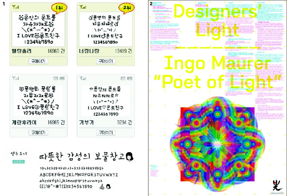
» (왼쪽부터)1. 에스케이(SK) 텔레콤과 애니콜의 휴대전화 서체. 2. 시각디자이너 성재혁의 작업. '조명디자인'에 집중한 전시에 맞춰 타이포로 빛의 배경을 표현했다.
"당신은 어떤 서체를 쓰십니까?"

'어떤 신용카드를 쓰고 어떤 아파트에 사는가'를 묻는 광고는 많다. 하지만 글자체와 당신의 관계를 묻는 질문은 많지 않다. 왜 그럴까. 특별히 시선을 끌지도 않을뿐더러 썩 중요한 질문이 아니기 때문이다. 하지만 한여름 공포영화의 타이틀이 '분홍빛' 샤방샤방한 표정을 하고 있었더라면 영화가 시작하는 순간 우리가 그토록 긴장했을까? 날카로운 선형에 새빨간 피를 흘리는 공포영화 서체나, 바위에 새겨진 '바르게 살자'의 굳건한 모습처럼 우리는 전달하려는 의미에 맞춰 '의도된' 글꼴 디자인 속에 살고 있다.

말하기 방식을 보완하는 하나의 수단

최근에는 젊은 세대를 중심으로 서체 디자인, 즉 타이포그라피(Typography)를 적극적으로 즐기는 분위기가 대세다. 그러면서 타이포그라피를 어떻게 봐야 하느냐는 태도와 인식의 중요성을 말하는 목소리도 늘고 있다. 이같은 변화는 아무런 맥락 없이 시작된 것은 아니다. 디자인 영역에서 '타이포그라피 비엔날레'와 타이포를 주제로 한 전시가 꾸준히 있었고 2~3년 전부터는 윤디자인, 산돌티움 등에서 개발한 휴대전화와 인터넷 서체가 일반인들의 소비욕을 자극했다.

잘 알려졌다시피 싸이월드 미니홈피에서는 수천가지 서체의 향연이 펼쳐진다. 휴대전화 기종에 따라 '폰트친구'(SK 텔레콤),'나만의 폰트'(KTF) 를 살 수 있고 윤디자인이 내놓은 스타의 손글씨를 이용한 '스타폰트'는 감성마케팅으로 자리잡았다. 서체개발 회사 '활자공간'의 대표 이용제씨는 "서체는 소비자들에겐 즐거운 유희이자 사적인 기호품"이라고 말한다.

젊은세대는 자기 느낌 따라 글꼴을 선별해 사용한다. 미니홈피는 아예 '손으로 사각사각' '또박또박 단순하게' '질감을 살린'의 이름으로 느낌별 카테고리를 선보여 '느낌'의 중요성을 활용했다. 재미있는 건 '하트봉봉 이효리체' '투명유리 꼬마체' '빈티지 그레이 퍼니체'와 같이 아기자기한 글꼴이 주를 이루며, 손으로 그려낸 듯한 유연한 이미지가 강조된다는 점이다. 이는 이미지와 문자를 활용한 창의적인 발상이 자유로운 타이포그라피의 강점을 십분 살린 것이다. 대학생 정지은씨는 "다른 서체로 글을 쓸 때마다 뉘앙스나 표현 문구 자체가 달라진다"며 "내 말하기 방식을 보완하는 하나의 수단"이라고 말한다. 레포트를 작성할 때도 명조체나 돋움체는 상투적으로 느껴져 피한다.


» (위에서부터 차례로) 3. 타이포그라피 디자인 국제 공모전 수상작. 4. 서울시가 개발한 '서울한강체'와 '서울남산체'. 5. 싸이월드의 '이니셜'은 사용자가 글꼴을 직접 꾸미는 디아이와이(DIY)서체다.
이런 변화 한가운데, 타이포그라피(typography)는 과연 어떤 의미일까? 여전히 전문 용어에 가까운 타이포그라피는 일반인들에겐 낯설다. 타이포그라피는 문자에 느낌을 불어넣는 전반적인 디자인 작업을 총칭한다. 애초 15세기 구텐베르크가 일군 활판인쇄술을 의미했지만 이젠 한글 디자인, 서체, 글꼴, 칼리그라피(calligraphy) 등 세부적인 디자인 영역이 하위개념으로 들어온다. 예술인 동시에 기술이고, 상상력인 동시에 상품이다.


근래 타이포그라피에 대한 관심 아래 다양한 문제제기가 나온다. 그 중 대표적인 것은 한글 디자인에 대한 관심이다. 우리나라 타이포그라피에서는 모국어인 한글에 대한 관심이 높을 수밖에 없다. 스스로를 '한글 디자이너'로 칭하며 '한글디자인연구소'를 꾸려왔던 이용제씨는 "이제 타이포그라피의 공공적인 측면에 주목할 때"라고 잘라 말한다. 그는 "글자는 아주 개인적인 동시에 공적인 이중적인 얼굴을 가졌다"며 공공기관에서 서체를 만드는 일은 세심한 사회적 관심이 필요한 공공재의 영역임을 지적한다. 이씨는 "만약 보기 싫은 글자체를 사회적으로 강요받는다면 얼마나 괴롭겠느냐"고 했다.

한옥구조의 곡선미에서 모티브를 얻다

실제 지난 7월15일 서울시에서 발표한 서울서체는 '한강'과 '남산'이라는 명칭으로 서울의 문화적 정체성을 내세워 이미지 만들기 효과를 노린 경우다. 발표된 서체는 명조계열인 서울한강체 2종과 고딕계열인 서울남산체 4종, 세로쓰기 1종으로 총 7종. 디자인서울총괄본부에 따르면 선비정신, 한옥구조와 기와의 곡선미에서 모티브를 얻었다. 지금은 서울시 현판, 보행자 안내 사인, 공문의 헤드라인에 시범 적용되고 있다. 디자인서울총괄본부 공공디자인담당관 권은선씨는 "서울시 글자체는 아직 수정 중인 현재진행형 글자"임을 강조한다. 해외의 경우 영국 런던의 뉴 존스턴 서체, 프랑스 파리 지하철 전용 파리지엥 서체처럼 도시경관에 시각적 질서를 부여한 사례가 있다. 잘 알려져 있지 않지만 우리나라에도 도에서 제작했던 '전라북도체'가 있다.

근래 타이포그라피의 양상은 지극히 사적인 차원과 공적인 차원에서 동시에 진행되는 것이 두드러진 특성이다. 타이포 전문가들은 "서체마다 최적화된 환경과 제 격에 맞는 꼴이 있기 마련"이라는 데 의견을 모은다. 보여주기 위한 '브랜드 만들기'가 아니라 다소 시간이 걸려도 기획 의도와 철학이 담긴 서체가 필요한 시점이라는 것이다. 이제껏 웹과 휴대전화, 한글 문서 공간 안에서 마음껏 서체를 고르는 선택의 자유가 주된 관심의 대상 이었다면, 사회적 차원에서 약속된 디자인을 공유하는 '공공디자인'으로서 타이포그라피를 볼 권리 또한 중요하다.

스위스에서 타이포그라피를 공부한 디자이너 박우혁씨는 서체를 새로 만들거나 다루는 모든 면에서 "가장 중요한 것은 글자를 대하는 태도"라고 말한다. 영화포스터에서 손글씨를 사용하는 등 몇년 전부터 타이포그라피를 향한 대중적인 관심은 분명 증가했다. 하지만 타이포그라피에 대한 인식은 다소 표피적이었다는 것이 그의 의견이다. 낱말 '가나다'를 컵이나 옷 표면에 새기는 것만이 한글을 사랑하고 글자를 잘 다루는 것은 아니다. 박씨는 "글자를 만드는 것, 다루는 것, 공간의 질서를 잡는 것 등 글자를 재료로 하는 다양한 태도가 있다"며 "부족함이 많은 서체도 사용 방식에 따라 가치가 달라질 수 있다"고 말한다.

정병규 강좌와 국제 공모전도 예정

글꼴에는 '느낌'이라는 경쾌한 차원이 있어 답답한 문단 사이 한줄기 빛이 되는가 하면, 서울시에서 진행중인 서체와 같이 '공동체의 얼굴'이라는 책임도 있다. 근래는 타이포그라피를 감상하고 공부할 기회가 끊이지 않는다. 문학과 지성사에서 운영하는 '문지문화원 사이'(02-323-4207)에서는 9월18일부터 북디자이너로 유명한 정병규의 '한글과 타이포그라피 강의'가 진행된다. 9월6일부터 삼원 페이퍼갤러리(02-468-9008)에서는 실험적인 타이포그라피 작업을 볼 수 있는 타이포그라피 디자인 국제 공모전 이 열린다.

현시원 기자 qq@hani.co.kr

기사등록 : 2008-09-03 오후 07:28:59 기사수정 : 2008-09-07 오전 11:40:13
한겨레 (http://www.hani.co.kr). 무단전재 및 재배포금지
- 출처: http://www.hani.co.kr/arti/specialsection/esc_section/308326.html

2008년 9월 5일 금요일

Emailing: 평판TV 두께경쟁 '진정한' 승자는

프린트하기 닫기

평판TV 두께경쟁 '진정한' 승자는
2008년 09월 04일 오후 19:04
권해주기자 postman@inews24.com

지난해부터 50㎜ 미만의 초슬림 TV 시제품들이 선을 보인 이후, 최근 시장에서 평판 TV 간 두께 경쟁이 치열하게 전개되고 있다.

지난 8월30일~9월3일 독일 베를린에서 열린 세계 최대 마케팅 중심 전자제품 전시회 'IFA 2008'은 두께를 중심으로 한 TV 업체들의 '디자인 경연장'을 방불케 할 만큼, 초슬림 경쟁으로 달아올랐다.

세계 TV 3대 기업인 삼성전자, 일본 소니, LG전자가 초슬림 액정표시장치(LCD) TV와 함께 두께를 줄일 수 있는 발광다이오드(LED) 백라이트 유닛(BLU) 기술을 중점 소개했다. 여기에 일본 샤프, 파나소닉과 유럽의 강자 필립스까지 두께 경쟁에 몰입하는 모습이었다.

지난해 IFA 2007과 올해 초 미국에서 열린 '소비가전전시회(CES) 2008'이 초슬림 TV 경쟁의 전초전이었다면, 이번 IFA 2008은 본격적인 시장에서 경쟁을 알리는 개막식과 같은 자리가 됐다.

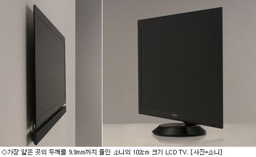
이번 전시회에서 두각을 나타낸 것은 가장 얇은 부분의 두께가 9.9㎜인 소니의 LCD TV '브라비아 ZX1'이었던 것으로 판단된다.

◆적정두께로 대형액자 스타일 연출…'무선연결 전쟁'도 대비


지난 2월 시장조사기관 디스플레이뱅크가 디스플레이 전문가 패널 77명을 대상으로 소니의 28㎝(11인치) 크기 발광다이오드(OLED) TV 'XEL-1'을 대상으로 한 심층조사는 흥미로운 결과를 나타냈다.

참여자들은 두께 3㎜의 XEL-1에 대해 두께가 가장 매력적(21%)이라고 응답했다. 3㎜ 두께에 대해선 적절하다는 응답이 83%로 대다수였으나, 나머지는 너무 얇고 부러지기 쉽다는 응답을 보이기도 했다. 즉 102㎝(40인치) 이상 대형 TV에선 무조건 얇은 게 좋지 않을 수 있다는 점을 유추해볼 수 있다.

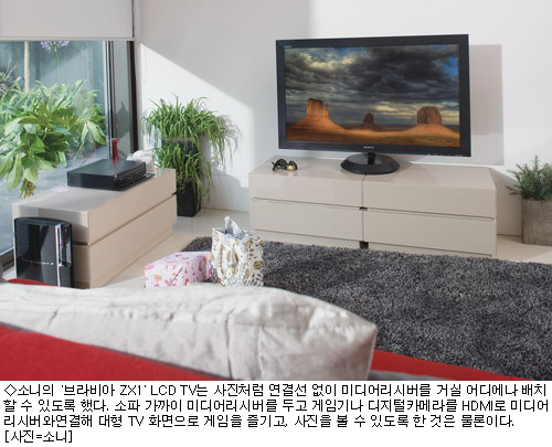
소니가 조만간 출시할 ZX1 LCD TV는 102㎝ 크기로 세울 수도 있고, 벽에 걸 수도 있도록 했다. 방송신호 수신을 위한 튜너는 무선으로 분리한 미디어리시버에 탑재했다. 지금까지 국내 삼성전자, LG전자는 해외 기업들의 튜너 분리형 초슬림 TV에 대해 부정적인 반응을 보였다.

튜너를 유선으로 분리하거나 받침대 부분에 탑재할 경우 두께는 얇아도 디자인 면에서 매력이 떨어진다는 이유에서였다. 삼성전자 임원은 "이러한 튜너 분리형 제품을 출시하지 않겠다"고 선언하기도 했다.


그러나 소니는 튜너를 무선으로 분리함으로써 디자인을 한층 강화할 수 있도록 했다. 미디어리시버를 30m 이내 거리에서 거실에 자유롭게 배치하면서도, 초고화질(풀HD) 방송을 수신하는데 무리가 없도록 한 것.

뿐만 아니라 고화질 멀티미디어 인터페이스(HDMI) 단자를 TV가 아닌 미디어리시버에 탑재함으로써 더 깔끔하고 간편하게 게임기, MP3플레이어, 캠코더 등을 TV와 연결해 사용할 수 있도록 한 점이 눈길을 끈다. TV를 시청하지 않을 때 USB메모리 등을 미디어리시버에 연결해 TV를 대형 디지털 액자로 활용할 수 있도록 한 것은 물론이다.

소니의 전략은 다가올 거실의 무선화를 미리 추구했다는 점에서 관심을 모은다. 무선 HDMI 및 무선 USB, 근거리 무선통신 기술 블루투스 등이 차츰 도입되면서 거실의 디지털기기들은 연결선 없이 통신을 하면서 고화질 영상들을 주고받는 시대가 열리고 있다.

이번에 박종우 삼성전자 디지털미디어총괄 사장이 무선 HDMI 솔루션을 준비하고 있다는 밝힌 것처럼, 거실의 '무선연결 전쟁'은 머지않아 달아오를 것으로 전망된다.

◆디자인·마케팅 기반 초슬림 TV 경쟁결과 주목


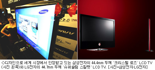
세계 TV 1위 기업인 삼성전자는 LG전자의 LCD TV(두께 44.7㎜)와 유사한 44.4㎜의 '크리스털 로즈' 디자인 초슬림 TV를 선보였다. 또 핵심고객들만을 대상으로 두께 9㎜ 미만의 132㎝(52인치) 크기 대형 초슬림 LCD TV도 보여줬다.

시장에서 초슬림 평판 TV 경쟁의 관건은 적절한 가격과 조화로운 디자인을 바탕으로 성공적인 마케팅을 진행할 수 있느냐 하는 것. 삼성전자가 올해 선보이고 있는 크리스털 로즈 디자인 TV, 앞면과 뒷면의 열정적인 검정과 빨강 색상이 조화를 이루는 LG전자의 '스칼렛' LCD TV는 프리미엄 제품이면서도 '제값'을 한다는 평가와 함께 국내·외에서 인기몰이를 하고 있다.

이러한 독특한 디자인에 초슬림이란 '무기'까지 더해지면서 국내 기업들이 슬림형 TV 시장경쟁에서 어느 정도 활약할지도 관심을 모은다.


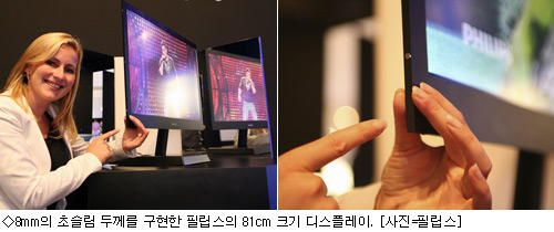
이번 IFA 2008에서 필립스는 LED를 적용해 두께가 8㎜에 불과한 81㎝(32인치) 디스플레이를 전시해 눈길을 끌었다. 그러나 크기가 작고 TV 튜너를 분리한 모니터 용도의 제품이란 점에서 향후 시장에서 가치에 대해선 의문시되는 상태.

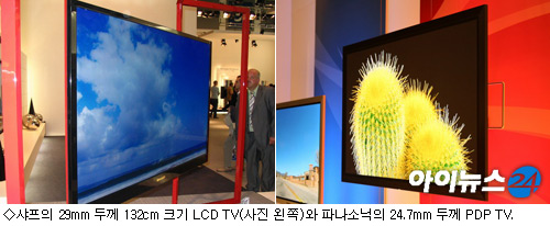
이밖에 샤프가 22~44㎜ 두께의 '아쿠오스 XS' 시리즈를 선보이며 동시에 제품 출시에 나섰다. 파나소닉은 CES 2008에 이어 24.7㎜ 두께 플라즈마 디스플레이 패널(PDP) TV를 전시하며, 가격 경쟁력을 갖춘 초슬림 PDP TV로 시장 공략에 나서겠다는 의지를 보였다.

LCD TV 기업들이 초슬림을 구현하기 위해 백라이트 유닛(BLU)으로 적용하고 있는 LED는 환경 친화적이면서 고화질, 고효율을 구현한다는 게 특징이다. 그러나 현재 널리 쓰이는 냉음극 형광램프(CCFL)보다 고가라는 게 단점.

3㎜ 두께의 소니 XEL-1처럼 LCD·PDP TV보다 한층 더 얇은 두께를 자랑하는 OLED TV 역시 높은 가격 때문에 대중화되진 못하고 있다. 초슬림 TV의 경쟁흐름이 가격과 디자인, 마케팅 등과 복합적으로 결합돼 전개되고 있는 가운데, 기업들의 제품판매 성적표가 어떻게 갈릴지 계속해서 관심을 모으고 있다.


IT는 아이뉴스24, 연예스포츠는 조이뉴스24
본 기사는 저작권법의 보호를 받으며 기사의 원형을 변형하거나 훼손하는 것을 금지합니다.
Copyright(c) . inews24.com All rights Reserved. Please read inews24's privacy policy.Contact us more information.


- 출처: http://itnews.inews24.com/php/news_view.php?g_serial=355547&g_menu=020800

2008년 9월 4일 목요일

‘박제가 되지 않은’천재를 아십니까?


.......................................................................................................................
'박제가 되지 않은'천재를 아십니까?
  10ㆍ11월 잇따라 한국무대 서는 사라 장ㆍ장한나
 

'은수저를 물고 태어난'바이올리니스트

프로스트ㆍ쇼펜하우어 즐겨 읽는 첼리스트…

천재 징크스 깨고 젊은 거장 반열에

1990년대 초중반 한국 클래식 음악계에 '천재 신드롬'을 몰고 왔던 바이올리니스트 사라 장(장영주.28)과 첼리스트 장한나(26)가 10월과 11월 잇따라 국내 무대에 선다.

솜털이 보송보송한 얼굴로 어른들을 깜짝 놀라게 했던 천재소녀들은 어느덧 20대 후반으로 접어들고 있다.

이제는 '젊은 거장'이라고 불러도 좋을 만큼 원숙미를 드러내며 자신의 입지를 굳혀가는 두 사람. 이들의 행로를 따라가 보는 것도 흥미롭지 않을까. ▶비슷하면서 다른 걸음 두 살 차인 사라 장과 장한나는 독일의 안네 소피 무터, 일본의 미도리 등에 비견되며 10대 이전에 이미 '천재 소녀'라 불렸다.

하지만 악기가 달라 두 사람이 나란히 비교된 적은 별로 없다.

둘 다 일찌감치 천재성을 인정받으며 세계적인 무대에 섰고, 미국 뉴욕에서 공부하며 그곳을 주 무대로 경력을 쌓아 갔지만 걸어온 길을 되짚어보면 비슷한 점만큼이나 다른 점이 많다.

사라 장은 1980년 미국 필라델피아에서 바이올리니스트 아버지와 작곡가 어머니 사이에서 태어났다.

3세 때 피아노를 배웠고, 4세 때 바이올린을 손에 잡았다.

사라 장은 누군가의 표현처럼 '은수저를 입에 물고 태어난' 탁월한 천재였다.

바이올린을 시작한 지 1년 만에 필라델피아 지역 오케스트라와 협연했고, 8세 때 마에스트로 주빈 메타와 리카르도 무티에게 발탁돼 뉴욕 필하모닉, 필라델피아 오케스트라와 각각 연주 및 레코딩 계약을 맺었다.

그리고 이듬해 링컨센터에서 열린 뉴욕필 신년음악회에서 공식 '데뷔'하면서 스타로 떠올랐다.

그 해에 사라 장은 자신보다 예닐곱 살 많은 언니오빠들과 함께 줄리어드 예비학교에 입학했고, 지도교수인 도로시 딜레이는 "사라 장처럼 놀라운 학생은 처음 본다"며 경이로움에 가까운 칭찬을 쏟아냈다.

또, 수많은 지휘자들이 "천재(Prodigy)"라는 감탄사를 연발하며 협연을 요청했다.

사라 장이 10대 초반에 이미 세계적인 명성을 얻은 배경에는 명지휘자들의 적극적인 후원이 있었다.

때문에 그는 단 한 번도 콩쿠르에 출전하지 않았지만 미처 감당하지 못할 만큼의 러브콜을 받았다.

사라 장을 아끼는 이들은 이런 바쁜 스케줄을 우려하기도 했다.

1993년 10월 3일자 뉴욕타임스에는 천재 소녀 사라가 엄청난 연주 스케줄 때문에 지치지 않을까를 걱정하는 장문의 기사가 실릴 정도였다.

한편, 장한나는 1982년 대한민국 수원에서 태어났다.

작곡을 전공한 어머니 덕분에 어려서부터 클래식 음악을 접했고, 6세 때부터 국내 '토종'으로 첼로를 배웠다.

그러나 장한나의 음악성이 남다르다는 것을 일찌감치 알아본 부모는 장한나가 11세가 될 무렵 미국으로 이주해 줄리어드 예비학교에 입학시켰다.

장한나는 사라 장과 달리 지휘자가 아닌 선배 연주자에 의해 발탁됐다.

1994년 현역 거장 첼리스트의 이름을 딴 로스트로포비치 콩쿠르에 출전해 쟁쟁한 성인 연주자를 물리치고 최연소 우승하며 세계 음악계를 놀라게 했고, 로스트로포비치는 장한나를 손녀처럼 아끼며 데뷔를 주선했다.

심사위원들은 "어린 소녀가 어떻게 인생의 온갖 고통과 슬픔을 음악에 표현해낼 수 있는지 놀랍다"며 충격 받았다.

콩쿠르 이전부터 이미 장한나의 천재성을 발견한 첼리스트 미샤 마이스키도 대가 없이 장한나의 후견인을 자처했다.

하지만 장한나는 사라 장과 조금 다른 길을 택했다.

어린 나이에 천재로 주목받은 연주자들이 중압감에 못 이겨 좌절하는 광경을 흔히 접한 스승들이 그에게 지나치게 과한 연주 일정을 잡지 말고 음악 외에 다양한 분야를 경험할 것을 권했기 때문이다.

덕분에 장한나는 사라 장처럼 어린 나이에 대단한 연주 경력을 쌓지는 못했지만 다방면으로 관심이 많고 지적인 연주자로 성장했다.

다른 연주자들처럼 음악학교에 진학하지 않고 하버드대 철학과에 진학한 것도 눈에 띄는 대목이다.

짬이 나면 프로스트와 쇼펜하우어를 즐겨 읽는다는 장한나는 음악 안팎으로 관심 분야가 다양하다.

지난해부터는 지휘자로서의 활동을 시작했고, 최근에는 바로크 음악을 탐구하고 있다.

수년 전, 일면식도 없던 가야금 명인 황병기를 찾아가 가야금을 배운 일화는 유명하다.

▶천재 징크스 극복, 성숙한 연주자로 일찌감치 전문 연주자로서 활동한 사라 장은 자의반 타의반 음악 외의 삶을 포기한 채 빡빡하게 살아왔다.

오죽하면 17세 때 연주 여행에 지쳐 매니저에게 당분간 쉬고 싶다고 하자, "앞으로 3년간의 스케줄이 꽉 짜여져 있기 때문에 3년 뒤에 쉬라"는 답을 들어야 했을 정도다.

어릴 때부터 삶의 대부분을 음악으로 채워서인지, 화려한 외모와 달리 일상에서는 모범생 타입인 것으로 알려져 있다.

그러나 자기 관리 능력이 뛰어나 한때 반짝하다가 조용히 퇴장한 일본의 천재 바이올리니스트 미도리와 달리 꾸준히 명성을 유지했다.

사라 장은 열정적인 보잉과 다소 과격한 무대 매너로 유명한데, 발을 구르거나 무대 위를 걸어다니며 한쪽 발을 앞으로 차는 제스처에 대해서는 호불호가 엇갈린다.

젊은 시절에는 파가니니, 차이코프스키, 시벨리우스 등 기교적이고 감성적인 작품을 주로 연주하고, 나이가 들면 차분하고 평화로운 브람스에 집중하고 싶다는 게 그의 음악적인 계획이다.

선배 첼리스트들의 보호 아래 성장한 장한나는 음악 외적인 부분에서 많은 아이디어를 취하며 탐험가 기질을 키웠다.

끊임없이 새로운 분야에 도전하는 것이 장한나의 특징이다.

사라 장은 한국어에 서툴지만 장한나는 어린 나이에 유학을 떠났음에도 한국어를 완벽하게 구사한다.

문장력과 언변이 뛰어나서, 신문에 칼럼을 기고하기도 하고 음악회에서 직접 작품 해설을 맡기도 한다.

장한나는 이제 겨우 26세지만 음악을 대하는 자세가 매우 성숙하고, 미래에 대한 꿈도 남다르다.

그가 밝힌 꿈은 로스트로포비치, 미샤 마이스키 등 훌륭한 스승으로부터 대가 없이 받은 사랑을 아이들에게 돌려주는 것. 자신이 지휘봉을 잡은 것도 그 꿈을 실현하기 위해 작은 첼로를 벗어나 가장 큰 악기이자 모든 악기의 결합체인 오케스트라를 연주하려는 것이라고 밝혔다.

그는 지난해 성남국제청소년관현악페스티벌에서 지휘자로 데뷔한 뒤 올해부터 베토벤 교향곡 전곡 연주를 계획하고 있다.

▶그들이 들려주고 싶은 이야기 먼저 내한하는 것은 사라 장이다.

7세 때 뉴욕필하모닉과 파가니니 바이올린 협주곡을 연주하면서 화려하게 데뷔한 뒤 세계 유수의 오케스트라 및 지휘자들과 호흡을 맞춰온 그는 이번에도 쟁쟁한 오케스트라를 대동한다.

10월 18, 19일 세종문화회관 대극장과 예술의전당 콘서트홀에서 열릴 내한 연주회에서 LA필하모닉 오케스트라와 함께 시벨리우스 '바이올린 협주곡'을 들려줄 예정. 지난 17년간 LA필을 이끌다가 이번 시즌을 끝으로 LA필을 떠나는 핀란드 출신의 에사 페카 살로넨이 지휘를 맡는다.

따라서 한국 관객에게는 에사 페카 살로넨의 고별 무대로서의 의미도 있다.

장한나는 11월 7일과 9일 세종문화회관 대극장과 예술의전당 콘서트홀에서 런던 체임버 오케스트라와 함께 비발디 첼로 협주곡을 연주한다.

런던 체임버 오케스트라는 영국에서 가장 오랜 전통을 가진 실내악 단체로, 호기심 많은 장한나의 바로크 음악 도전기를 접할 수 있는 기회다.

김소민 기자(som@heraldm.com)


2008.09.04


Copyright 2001 ~ 2004 Herald Media INC. All rights reserved.
 

Intel aims x86 at digital TVs

Aug. 20, 2008

Intel will ship a Pentium M-based system-on-chip (SoC) for consumer devices like networked optical players, set-top boxes, and digital TVs. The 800MHz Media Processor CE3100 ("Canmore") aims to bring YouTube and other PC-based entertainment platforms to home entertainment systems, where today MIPS-based SoCs from Sigma, Broadcom, and others dominate.

Intel calls the CE 3100 "the first in a new family" of SoCs aimed at the consumer electronics segment. More specifically, it targets network-enabled optical drives and set-top boxes, where today MIPS is probably the dominant architecture, thanks to popular offerings from Sigma, Broadcom, and others. Intel appears to be hoping that x86's better support for the software needed to run YouTube and other PC-based entertainment platforms will help it compete, as the PC and CE markets continue to converge.


Canmore function block diagram
(Click to enlarge)

Touted Canmore features include:

  • High-definition video support
  • "Home-theater quality" 7.1 audio
  • 3-D graphics
  • Multi-stream video decoding and processing hardware
  • Dedicated multi-channel dual audio DSPs
  • 3-D graphics engine enabling advanced UIs and EPGs
  • USB 2.0 and PCI Express expansion
  • Intel Media Play:
    • Hardware MPEG-2, H.264, and VC-1 decoders, for broadcast TV and optical media
    • Software codecs for "Internet content" (for greater flexibility)
Specifications listed by Intel include:
  • 800MHz Core Frequency
  • 256K 2-way set-associated L2 cache
  • 100/133MHz FSB
  • 800MHz Core Frequency
  • PowerVR SGX535 3D/2D graphics and video accelerator at 216MHz
  • 3-channel 32-bit DDR2 memory controller supports memory sizes from 64MB to 3GB
  • 250MHz RISC-based video co-processor
  • Dual 340Mhz DSP cores programmed in microcode for audio operations:
    • Audio decode (DD+, DTS-HD, AC3, AAC, MP3, WM, Lossless)
    • Audio encode (AC3, DTS)
    • Audio effects, resampling, mixing
  • HDMI audio support including high-bit rate (HBR) audio
  • 5 x I2S outputs for 7.1 channel audio + stereo audio outputs
  • 1 x S/PDIF output
  • 24-bit 192KHz audio support
  • Configurable 10-stage graphics pipeline supporting dual 1080i@60 input, and 1.5x 1080p@60 output
  • HDMI/DVI 1.3a compliant video interface with support for 1080p, 36-bit deep color in RGB/YUV
  • Video output composition hardware
  • Peripherals
    • 2 USB 2.0 host ports
    • Ethernet 802.3 10/100/1000 MAC with RGMII/RMII interface
    • 2 x SATA-150
    • 2 x single lane PCI Express ports
    • IR remote support
    • 3 x I2C interfaces with 1 additional dedicated for DDC (HDMI)
    • 1 x SPI Interface with 4 chip-selects
    • 2 x UARTS, one with hardware handshake signals for modem connectivity
    • Configurable parallel expansion bus with 4 chip-selects
    • NOR flash boot interface
    • 16 x GPIO pins (8 dedicated: other pinmuxed)
    • Timers, RTC
  • Other feature:
    • 250MHz system clock
    • Unified Memory Architecture (UMA)
    • PCI mapped internal devices
    • Legacy and MSI (message based) interrupt support
    • Coherent Data path for control and non-coherent data path for bulk video data
    • IEEE 1491.1 complaint JTAG
    • 609 signal pins in a 37.5mm lead free FC-BGA7 (1434 balls) package

Eric Kim, GM of Intel's digital home group, stated, "The Web is quickly moving to the TV. [The CE 3100 is our] first IA SoC with Internet compatibility for consumer electronics devices."

Canmore appears to be Intel's second x86-based SoC, and its first for consumer electronics devices. The company earlier shipped the EP80579 ("Tolapai"), also based on a Pentium M core, and targeting storage applications.

Intel based previous CE-series chips, such as the CE 2110, on the ARM architecture.

System-on-chip processors typically integrate a CPU core with memory and storage controllers, display controllers, on-chip peripheral interfaces, and specialized hardware subsystems such as security co-processors, all on the same physical die.

Availability
The CE 3100 will ship next month. Early customers reportedly include Samsung and Toshiba. Pricing was not stated.

--------------------------------------------------

- 출처: http://www.linuxdevices.com/news/NS2494568985.html

2008년 9월 3일 수요일

전자 메일 보내기: 우주정거장에서 촬영... 지구의 끝에서 빛나는 야광운

 
우주정거장에서 촬영... 지구의 끝에서 빛나는 야광운


1일 해외 과학 매체들은 지난 여름 국제우주정거장에서 기이하고도 아름다운 구름 사진이 촬영되었다고 전했다. 지구의 대기권과 우주 공간의 경계 사이에서 빛나는 얇고 긴 푸른색 구름은 '야광운'이다.


고도 76~85km에서 나타나는 이 구름은 120년 전 처음 관측되었으나 여전히 완전한 과학적 설명은 없는 실정이다.


야광운이 나타나는 곳의 대기는 극도로 건조하다. 사하라 사막보다 1억 배 가량 건조하다는 것이 해외 언론의 설명. 이 구름은 어디에서 수증기를 얻을까. 열대의 상승 기류 혹은 산화 메탄이 수증기의 원천일 것으로 추정된다.


(사진 : 지난 7월 22일 일출전 국제우주정거장이 서부 몽골을 지날 때 촬영했다 )


김경훈 기자
- 2008년 9월 2일(화) 10:00 [팝뉴스]