|
2010년 4월 29일 목요일
Parallel Engines Launches World’s Largest Semiconductor-IP Directory for FPGA

Xilinx Unveils ARM-Based Processing Architecture for Delivering Unrivaled Levels of Performance in Embedded Systems
press release
April 27, 2010, 5:00 p.m. EDT
Xilinx takes processor-centric approach to deliver platform that combines the best of serial and parallel processing
![]()
SAN JOSE, Calif., April 27, 2010 /PRNewswire via COMTEX/ -- Embedded Systems Conference -- Xilinx Inc. /quotes/comstock/15*!xlnx/quotes/nls/xlnx (XLNX 26.54, +0.24, +0.91%) today introduced the architecture for a new Extensible Processing Platform that will deliver unrivaled levels of system performance, flexibility and integration to developers of a wide variety of embedded systems. The ARM(R) Cortex(TM)-A9 MPCore(TM) processor-based platform enables system architects and embedded software developers to apply a combination of serial and parallel processing to address the challenging system requirements presented by the global demand for embedded systems to perform increasingly complex functions.
The Xilinx(R) Extensible Processing Platform offers embedded systems designers a processor-centric design and development approach for achieving the compute and processing horsepower required to drive tasks involving high-speed access to real-time inputs, high-performance processing and complex digital signal processing -- or any combination thereof -- needed to meet their application-specific requirements, including lower cost and power.
"Today's embedded software developer is being tasked to build complex applications that require tremendous levels of system performance, and they need to deliver that performance within tightly managed cost, schedule and power budgets," said Vin Ratford, Xilinx Senior Vice President for Worldwide Marketing and Business Development. "By creating an architecture within a familiar ARM processor-based development framework, this new Extensible Processing Platform can be the engine of innovation for many design teams held back today by performance bottlenecks."
A software-centric development flow is enabled by a processor-centric approach which presents a full processor system - including caches, memory controllers and commonly used connectivity and I/O peripherals - that boots and can run a variety of operating systems (OS) at power-up, such as Linux, Wind River's VxWorks and Micrium's uC-OSII. The ARM architecture and its Connected Community ecosystem further maximize productivity for developers of embedded systems, while unrivaled performance is achieved by Xilinx's architecting the subsystem around ARM's dual-core Cortex(TM)-A9 MPCore(TM) processors, each running at up to 800 MHz, combined with the parallel-processing capabilities of Xilinx's high-performance, low-power 28-nanometer programmable logic. The programmable logic is tightly coupled with the processor system through the high-bandwidth AMBA(R)-AXI(TM) interconnects to accelerate key system functions by up to 100x, using off-the-shelf and/or custom IP. This architectural approach addresses common performance bottlenecks between these parallel and serial computing environments, memory and I/O. It also gives the processor system configuration control of the programmable logic, including dynamic reconfiguration.
"Taking advantage of the parallelism of programmable logic is an excellent method for overcoming cost and power challenges in systems that require significant levels of high performance," said Simon Segars, President ARM Inc. "Xilinx's new architecture abstracts much of the hardware burden away from the embedded software developers' point of view, giving them an unprecedented level of control in the development process."
Software developers can leverage their existing system code based on ARM technology and utilize vast off-the-shelf open-source and commercially available software component libraries. Because the system boots an OS at reset, software development can get under way quickly within familiar development and debug environments using tools such as ARM's RealView development suite and related third-party tools, Eclipse-based IDEs, GNU, the Xilinx Software Development Kit and others.
Unrivaled Performance to Enable New Applications
Demand for higher levels of embedded system performance is being driven by end market applications that require multifunctionality and real-time responsiveness, such as automotive driver assistance, intelligent video surveillance, industrial automation, aerospace and defense, and next-generation wireless. In the automotive sector alone, with greater than 50 million cars produced each year, and an estimated 600 million motor vehicles on the road, today's $1.3-billion-dollar driver assistance market is expected to grow to $5.8 billion by in 2017(1) as manufacturers deploy more embedded systems in their vehicles to make them safer.
With statistics showing that 60 percent of front-end collisions could have been avoided with an extra .5-second response time, or that driver fatigue accounts for an estimated 30 percent of all driver fatalities, the motivation to leverage technology to save lives is clear. As developers of driver assistance systems pack more compute power into their applications, radar and infrared sensors, cameras and other system components must be installed into confined spaces within the automobile. The new Xilinx Extensible Processing Platform offers a single-chip solution for optimizing application-specific hardware/software partitioning and accelerating functions in hardware to drive complex algorithms. This enables customers to further differentiate their embedded systems to gain a competitive advantage in their markets.
In a market expected to reach $46 billion by 2013(2), developers of new intelligent video technologies need processing platforms for building applications that can automatically monitor video patterns and body language, combined with audio, to make intelligent decisions and send alerts, thus reducing the chance for errors. The technology is already moving to full high-definition video and frame rates up to 60 frames per second, but current solutions do not offer sufficient compute power for image processing and advanced analytic functions. The dual Cortex-A9MPCore-based processor system, coupled with the massive parallel-processing capabilities of the programmable logic, enables this capability. Developers also gain an opportunity for innovative algorithm design, scalability and field upgradability within a familiar ARM-based design environment.
Wireless telecommunication is being driven by the need for lower power, smaller physical form factors and reduced development costs, to support an ever-increasing number of users and data-hungry applications. New technologies such as 4G LTE (Long-Term Evolution) can address bandwidth requirements, but smaller, more efficient base stations are essential to meeting overall market requirements. The Xilinx Extensible Processing Platform will help developers of next-generation wireless base stations to meet these needs by providing high-bandwidth parallel processing of 4G signals in combination with multiuser data management on Cortex A9 processors - all in a small, power-efficient, cost-effective integrated solution. Because the platform is extensible, developers have the flexibility to implement future equipment updates and performance upgrades of both hardware and software.
The new Extensible Processing Platform is part of Xilinx's Targeted Design Platform strategy, which provides customers with market- and application-specific environments that are easy to use, enabling them to evaluate and understand technology, and finally provide application platforms that can be modified and extended to accelerate their development time and focus on differentiation. Xilinx has also engaged with ARM Services to provide detailed ARM Cortex-A9 hardware training for design teams and field application engineers who will be supporting the eventual product rollout.
Visit the Xilinx booth (#1716) at the Embedded Systems Conference to see and learn more. Pricing and availability will be announced for products based on the Extensible Processing Platform architecture in early 2011. Visit www.xilinx.com/technology/roadmaps and click the link to "Be the First to Know" for product details, as they become available.
About Xilinx
Xilinx is the world's leading provider of programmable platforms, with more than 50 percent market share in the programmable-logic device (PLD) segment of the semiconductor industry. For more information, visit www.xilinx.com.
#1023P
XILINX, the Xilinx Logo, and other designated brands included herein are trademarks of Xilinx in the United States and other countries. All other trademarks are the property of their respective owners.
(1) Intelligent Car Initiative- Europe's Information Society; International Organization of Motor Vehicle Manufacturers; http://www.worldometers.info/cars/
(2) Multi-media Intelligence Report - April 2008
    Editorial Contact:
    ------------------
    Bruce Fienberg
    Xilinx, Inc.
    408-879-4631
    bruce.fienberg@xilinx.com
SOURCE Xilinx, Inc.
Copyright (C) 2010 PR Newswire. All rights reserved.
==========
Xilinx hardwires Cortex-A9 MPCore processor into FPGA
Richard Wilson
Tuesday 27 April 2010 22:01
Xilinx has introduced its first FPGA design platform with an embedded ARM Cortex-A9 MPCore processor.
Xilinx has worked with ARM for over a year to allow the programmable logic elements of the FPGA, with their highly parallel architecture, to be closely coupled with the processor system through the AMBA-AXI on-chip bus.
According to the FPGA supplier, this architectural approach “addresses common performance bottlenecks between these parallel and serial computing environments, memory and I/O.”
“It also gives the processor system configuration control of the programmable logic, including dynamic reconfiguration,” said Xilinx.
“By creating an architecture within a familiar ARM processor-based development framework, this new Extensible Processing Platform can be the engine of innovation for many design teams held back today by performance bottlenecks,” said Vin Ratford, Xilinx senior v-p for worldwide marketing and business development.
The processor subsystem is based around ARM’s dual-core Cortex-A9 MPCore processors, each running at up to 800MHz.
The aim has been to offer within the FPGA a full processor system including caches, memory controllers and commonly used connectivity and I/O peripherals.
Efforts have also been made to support different operating systems such as Linux, Wind River’s VxWorks and Micrium’s uC-OSII.
The aim is to allow developers to tap into off-the-shelf open-source and commercially available software component libraries.
“Because the system boots an OS at reset, software development can get under way quickly within familiar development and debug environments using tools such as ARM’s RealView development suite and related third-party tools, Eclipse-based IDEs, GNU, the Xilinx Software Development Kit and others,” said Xilinx.
The AMBA-AXI bus protocol has been redesigned to make it compatible with highly parallel embedded FPGA design. It adds support for longer bursts which will support devices with large block transfers.
There is also quality of service (QoS) signalling to manage latency and bandwidth in complex multi-master systems.
“This will take embedded system design to performance and efficiency levels considered the exclusive domain of desktop, laptop and network equipment,” said Keith Clarke, v-p and general manager of fabric IP processor division at ARM.
The first FPGAs based on what the company is calling the Extensible Processing Platform will be available next year.
See: Xilinx brings ARM Cortex and AMBA to its FPGAs
==========
NEWS ANALYSIS - Xilinx puts ARM core into its FPGAs
New embedded systems architecture employs ARM core in processor-centric FPGAs.
By Richard Nass
(04/27/10, 05:00:00 PM EDT)
My first reaction was, "It's about time." My second reaction was, "I hope they did it right." Let me explain. Xilinx, considered by many to be the market leader for FPGAs, had a hole in its lineup, at least in my eyes. For at least a couple of years, I asked the folks at Xilinx why they weren't making a serious run at ARM-based FPGAs.
I learned that it wasn't as simple as dropping the core into the company's library. There were It actually took some design issues that needed to be overcome to ensure that the ARM core could operate at its maximum efficiency. Those changes were put in place last fall, when Xilinx announced a technology agreement with ARM.
Essentially, the technology agreement revolved around changes made to the AMBA bus to keep the programmable logic tightly coupled with the processor core. Xilinx adopted ARM physical IP, and the two companies made a technical commitment to work together to define the AMBA 4 specification, which is the de-facto industry standard for on-chip communications on SoCs designed with an ARM core.
With that technology in place, it was clear where Xilinx was headed. However, there were a few details on which Xilinx remained mum. As of today at the Embedded Systems Conference Silicon Valley, that silence is broken and all questions are being answered. They're calling it their Extensible Processing Platform that takes advantage of ARM's dual-core Cortex-A9 MPCore processors, each running at up to 800 MHz. With the platform, designers can apply a combination of serial and parallel processing for applications that require high-speed access to real-time inputs, high-performance processing, and/or complex digital signal processing.

Thanks to the changes made in the architecture, a software-centric development flow is enabled by the processor-centric approach which presents a full processor system. This includes caches, memory controllers, and commonly used connectivity and I/O peripherals. It's built using Xilinx's high-performance, low-power 28-nanometer technology.
The high-bandwidth AMBA-AXI interconnects keep the programmable logic tightly coupled with the processor core. This architectural approach addresses common performance bottlenecks between these parallel and serial computing environments, memory, and I/O. It also gives the processor control of the programmable logic, including dynamic reconfiguration.
The architecture abstracts a lot of the hardware burden from software developers, who can now tap into the vast off-the-shelf open-source and commercially available software component libraries. Another key feature is the FPGA's ability to boot an operating system (OS) at reset.
Pricing and availability will be announced for products based on the Extensible Processing Platform architecture in early 2011.
==========
출처: http://www.embedded.com/products/integratedcircuits/224600510
2010년 4월 28일 수요일
묻지마식 무선랜 접속은 금물
![]()
해커 덫에 걸리기 십상...보안 10계명 생활화
2010년 04월 27일 (화) 18:26:27 / 장윤정 기자 linda@etnews.co.kr

▲ 무선랜은 접속이 손쉬운만큼 해킹, 개인정보유출, 분산서비스거부(DDoS) 공격 등 악의적인 공격의 표적이 되기 쉽다. 사진은 G밸리에 근무하는 직원들이 무선랜을 즐기는 모습.
‘수년전 H은행과 유사한 가짜 사이트를 통해 금융거래에 필요한 개인정보를 알아낸 뒤 12명으로부터 1억2000여만원을 가로챈 일당 3명이 구속된 바 있다. 당시 이들은 피싱 사이트 제작·설치부터 계좌에서 돈을 빼내는 모든 범행 과정에서 IP 추적이 어려운 무선랜을 이용했다.’
웬만한 대형 오피스 빌딩에 들어가면 무선랜 AP(Access Point)에 손쉽게 접속할 수 있고 공짜로 무선랜을 이용하는 등 무선랜 사용이 급속히 늘고 있다.
접속이 손쉬운 만큼 무선랜은 H은행 피싱 사이트 사고처럼 해킹·개인정보유출 (DDoS) 공격 등 악의적인 공격의 루트가 되기도 싶다.
방송통신위원회는 이러한 이유로 지난해 하반기 무선랜 공유에 대해 보안 문제를 이유로 AP에 암호와 패스워드 설정을 의무화하는 등 통신사업자와 사용자의 보안 의무를 강제화하는 법 제정 방안을 검토하기 위해 연구용역을 의뢰한 상황이다.
그러나 법 시행 여부를 떠나 사용자의 올바른 무선랜 사용이 금전 및 개인정보유출 사고를 막는 지름길이다.
커피숍·호텔 등 공공시설에 설치된 무선랜은 이용자 편의성을 우선하기 때문에 개인 ID 입력 등 이용자 확인만을 제공하고 암호설정을 하지 않는 경우가 많다. 암호 설정을 하지 않는 무선랜 환경에서는 개인정보 유출 등 피해의 우려가 있다.
특히, 인터넷뱅킹 등 민감한 애플리케이션 서비스는 사용하지 않는 것이 좋다. 자칫 개방된 무선 AP에 함부로 접속했다가 개인정보·금융정보 등의 불법 데이터 수집을 목적으로 피싱용 무선 AP를 설치하고 접속을 유도하는 해커들의 덫이 기다리고 있기 때문이다.
무선랜 사용자 인증과 암호화는 필수로 설정해야 하지만 무선 AP도 보안 관리해야한다. 무선 AP의 신호 세기를 줄여 필요 이상으로 넓은 범위까지 접속이 가능하도록 설정하지 않는 게 좋다. WPA-PSK 등 최신 암호기법을 이용해 노출되기 어려운 암호를 설정해야한다.
또한 무선 AP의 이름을 나타내는 SSID(Service Set IDentification)의 숨김 기능이 가능한지도 살펴봐야한다. SSID를 비공개로 하면 외부인이 무선공유기(AP) 존재유무를 확인할 수 없어, 무단 사용을 막을 수 있다.
그리고 무선AP를 사용하지 않는 시간에는 전원을 차단해 무단 접속을 막는 것도 중요하다. 외부 접속시 내 컴퓨터를 안전하게 보호하기 위해 운영체제에 기본 장착된 개인방화벽을 항상 켜둬야 한다.
스마트폰 사용시에도 무선랜 접속시 안전을 위해 스마트폰 백신 등을 설치해 악성코드, 바이러스 등을 진단치료해야 하고 블루투스는 사용시에만 활성화, 감염 위험을 낮춰야한다.
심종헌 유넷시스템 사장은 “스마트폰·인터넷 전화 등 무선랜 사용이 늘어감에 따라 안전하게 무선 인터넷을 이용하기 위해서는 사용자 스스로 무선 접속에 대한 관리가 필요하다”며 “해커에게 개인정보나 기업의 주요 데이터를 도난당하지 않기 위해서는 생활속에서 무선랜 사용 수칙을 제대로 지켜야 한다”고 말했다.
◇ 안전한 무선랜 사용 10계명
- 무선랜 사용자 인증과 암호화를 반드시 설정한다.
- 보안설정이 힘든 오래된 무선AP는 가능한 교체한다.
- 암호없는 무선랜 사용시에는 금융정보 등 주요정보 송수신은 삼간다.
- 와이파이 형태의 무선인터넷전화기 사용시 통신사업자가 제공하는 기본암호키를 반드시 변경, 설정한다.
- 무선AP의 전파 신호는 필요한 범위 내로 설정한다.
- AP의 이름을 나타내는 SSID를 숨기고 WPA-PSK 등 최신 암호화 기술을 사용해 공유기 무선 보안 관리를 철저히 해야 한다.
- 사용하지 않을 경우 AP의 전원을 차단한다.
- 무선랜 패스워드는 쉽게 추측하기 어려운 영문, 숫자의 조합으로 설정하며, 패스워드는 주기적으로 교체한다.
- 자신의 무선랜 접속계정이 다른 사람에게 노출되지 않도록 철저히 관리한다.
- 무선노트북의 개인방화벽을 설치, 항상 활성화시켜두어야하며 스마트폰에도 개인정보 유출을 방지하는 관리프로그램을 설정해둔다.
ⓒ 보안닷컴(http://www.boan.com) 무단전재 및 재배포금지 | 저작권문의
==========
2010년 4월 27일 화요일
Silego Technology Introduces GreenPAK: A Micro-FPGA with Programmable Analog
Earthtimes.org (Press Release)
Silego Technology Introduces GreenPAK: A Micro-FPGA with Programmable Analog
Posted on : 2010-04-26 | Author : Silego Technology, Inc.
News Category : PressRelease
SANTA CLARA, Calif. - (Business Wire) Silego Technology, Inc. announces the GreenPAK. GreenPAK is a 2x2 mm TDFN one-time programmable micro-FPGA with configurable analog components. GreenPAK (logic & analog) has been designed to operate as a stand alone IC capable of performing many 4-bit and 8-bit microcontroller applications or work in conjunction with Silego’s GreenCLK (timing) and GreenFET drivers (power sequencing) product lines to remove up to 25% of all components on larger computation and communication system boards.
GreenPAKs are configured with GreenPAK Designer 1.0 software and a USB-based GreenPAK programmer. The software is intuitive and its configuration requires no programming language or complier allowing a designer to configure, program, and test their custom GreenPAK in minutes.
GreenPAK, as a stand alone product, is targeted at many 4 and 8-bit microcontroller applications. The on-board finite state machine, logic, counters, delays, ADC, voltage reference, oscillator, and PWM allow for 1000’s of applications such as interface to sensors of all types, LED drivers, motor controllers, touch sensing, and over voltage protection.
GreenPAK is also the logic and mixed signal element of Silego’s Green product strategy for large computation and communication system boards. GreenPAKs remove power on resets, temperature sensor interface ICs, delay or timing related logic, glue logic, and power good circuits.
“Silego’s GreenPAK products are the first ICs that are able to cost effectively remove massive numbers of passive and simple active components from PCB designs improving reliability and reducing procurement issues while saving board area, power, and cost,” said John McDonald, Vice President of Marketing and Sales at Silego. “The success of the GreenPAK and its sibling, the GreenSAK product family, contributes to Silego’s vision of providing a comprehensive suite of ICs that clean up every PCB by reducing component count, simplifying design, and saving power and board space.”
Silego provides many options to learn about GreenPAK through live video web support 16 hour per day, training videos, software, or by scheduling one-on-one training session with a Silego application engineer to assist with GreenPAK development.
Prices and Availability
GreenPAK products are in volume production. Samples, datasheets and demonstration boards are available at www.silego.com. GreenPAK products are priced from $0.15 to $0.25 in moderate volume. Please contact Silego for ultra-high volume pricing.
About Silego
Silego Technology, Inc., founded in 2001, is recognized with the Deloitte Technology Fast 50 Rising Star ranking as one of the fastest growing technology companies in the Silicon Valley. Silego develops silicon solutions to reduce part count, power, and cost. Silego is the world’s largest notebook and netbook clock supplier and has numerous product lines that cover DDR3 register ICs, Consumer ICs, Notebook and Netbook ICs. Silego is headquartered in Santa Clara, California, with operations and design centers around the globe. Silego Technology is privately owned and backed by leading venture capital firms.
Silego Technology, Inc.
Tania Hryhorenko, 408-327-8800
Inside Sales Associate
taniah@silego.com
Press Release Print Source :
http://www.earthtimes.org/articles/show/silego-technology-introduces-greenpak-a-micro-fpga-with-programmable-analog,1266643.shtml
© 2010 earthtimes.org. All Rights Reserved.
This material may not be published, broadcast, rewritten, or redistributed.
Dust Networks Announces ARM Cortex-M3 Processor Based IEEE 802.15.4 SOC
![]()


D&R Headline News | Most Popular | SoC News Alerts | ![]() |
| ![]()
Dust Networks Announces ARM Cortex-M3 Processor Based IEEE 802.15.4 SOC
New benchmark for ultra-low power wireless sensor network performance
Hayward, CA, (April 26, 2010)--Dust Networks®, the leading supplier of wireless sensor networks (WSN), today announced that its new IEEE 802.15.4 products will include the powerful, low power ARM®Cortex™-M3 processor. Dust Networks' new family of system-on-chips (SoCs) will be the basis for a variety of upcoming standards-based WSN products, including IEC 62591 (WirelessHART™), 6LOWPAN (IP), and Zigbee ®PRO products that will provide unprecedented low power consumption while delivering a compelling set of energy saving, high performance features including:
- A 32-bit ARM Cortex M3 processor and rich interfaces enable a powerful computing platform while conserving power.
- The world's lowest power IEEE 802.15.4 radio: a new benchmark is set, with a mere 3 mA transmit at 0 dBm and 3 mA receive current, delivering 5-10 times the battery life of competing technologies, and further expanding the applicability of energy harvesting power sources.
- Extended range capabilities, with up to 8 dBm output power on-chip PA and an optional external power amplifier.
- The industry's first IEEE 802.15.4E-ready product, incorporating the emerging standard for time synchronization and channel hopping, while providing legacy support for 802.15.4-2006.
"Our new SoCs are geared to deliver the highest performance while running at a fraction of the power of competing silicon," said Dr. Kris Pister, Chief Technologist at Dust Networks. "In selecting the ARM Cortex-M3 processor for our SoC, we did not have to trade-off performance for power. Dust Networks new IEEE 802.15.4 SoCs will require less than one-tenth of the energy per operation of comparable SoCs."
The level of systems integration in the SoCs is very high, including on-chip power amplifier, DC-to-DC converter, 10 bit ADC and a built in temperature sensor. With configurations up to 512kB of flash and 72kB of RAM, these SoCs will have both the highest computational horsepower of any 802.15.4 chip on the market, and the lowest power consumption. In doze mode, with full processor state and RAM retention, current consumption is under 1uA.
"Dust Networks' adoption of the ARM Cortex architecture is a clear demonstration of the growing support for ARM Cortex-M3 processor-based for low-power applications " said Eric Schorn, VP marketing, Processor Division, ARM. "The ARM Cortex-M3 CPU is ideal for battery operated or energy harvesting designs where performance really matters and the feature-filled Dust SoC is a powerful example of what can be done with a 'green' approach to SoC design, in applications where every nanoamp counts. "
"Low power radios such as IEEE 802.15.4 and wireless mesh networking, epitomized by Dust Networks' TSMP protocol and its "Smart Dust" roots, have transformed the industrial wireless sensor network landscape" said Mareca Hatler, ON World research director. "With the introduction of ultra low power versions of SmartMesh IP (6LoWPAN) systems and ZigBee products, Dust Networks will expand the growing number of "Smart World" applications that span Smart Buildings, Cities, Government and Homes."
About Dust Networks
Dust Networks, the leader in standards-based intelligent wireless sensor networking (WSN), provides ultra low-power, highly reliable systems to OEMs. Dust Networks wireless technology enables unprecedented access to information from the physical world, in markets that range from industrial monitoring and control to emerging markets such as the Smart Grid, Smart Cities and Smart Buildings. Dust Networks' embedded products combine extremely low-power RF System-on-Chip (SoC) technology with revolutionary wireless networking capabilities, providing OEMs with a full range of standards-based WSN solutions that are flexible and easy to integrate. Dust Networks partners with industry and standards groups such as the HART Communication Foundation, IEEE, IETF, IPSO, ISA, SunSpec Alliance and the Zigbee Alliance to ensure the broad adoption of interoperable wireless sensor networking products.
About ARM:
ARM designs the technology that lies at the heart of advanced digital products, from wireless, networking and consumer entertainment solutions to imaging, automotive, security and storage devices. ARM's comprehensive product offering includes 32-bit RISC microprocessors, graphics processors, video engines, enabling software, cell libraries, embedded memories, high-speed connectivity products, peripherals and development tools. Combined with comprehensive design services, training, support and maintenance, and the company's broad Partner community, they provide a total system solution that offers a fast, reliable path to market for leading electronics companies. More information on ARM is available at http://www.arm.com

All material on this site Copyright © 2009 Design And Reuse S.A. All rights reserved.
==========
출처: http://www.design-reuse.com/news/23242/arm-cortex-m3-processor-ieee-802-15-4-soc.html
2010년 4월 22일 목요일
Timing Closure on FPGAs
![]()
![]()
April 22, 2010
Sleep peacefully at night knowing that your design is in tip-top shape
By Nelson Lau, Spirent Communications
Have you ever written code that behaves correctly under a simulator only to have intermittent failures in the field? Or maybe your code no longer functions properly when you compile with a newer version of your tool chain. You review your test bench and verify 100 percent complete test coverage and that all tests have passed with no errors--yet the problem stubbornly remains.
While designers understandably place great emphasis on coding and simulation, they often have only a nodding acquaintance with the internal workings of the silicon within an FPGA. As a result, incorrect logic synthesis and timing problems, rather than logic errors, are the cause of most logic failures.
But writing FPGA code that creates predictable, reliable logic is simple if designers take the right steps.
In FPGA design, logic synthesis and related timing closure occur during compilation. And many things, including I/O cell structure, asynchronous logic and timing constraints, can have a big impact on the compilation process, varying results with each pass through the tool chain. Let's take a closer look at ways to eliminate these variances to better and more quickly achieve timing closure.
The I/O Cell Structure
All FPGAs have I/O pins that can be highly customized. The customization affects timing, drive strength, termination and many other factors. When your I/O cell structure is not clearly defined, your tool chain will often use a default that may or may not be what you want. In the VHDL code below, the intent is to create a bidirectional I/O buffer named sda using the declaration "sda: inout std_logic;".

When the synthesis tool sees this block of code, there is no clear directive on how to implement the bidirectional buffer. As a result, the tool will take a best guess.
One way to accomplish the task would be to use a bidirectional buffer on the I/O ring of the FPGA (indeed, this is the desired implementation). Another option would be a tristate output buffer and input buffer, both implemented in lookup table (LUT) logic. A final possibility would be to use a tristate output buffer on the I/O ring along with an input buffer in an LUT—and this is the option that most synthesizers will choose. All three methods yield valid logic, but the last two implementations result in additional routing delays when the signal moves between the I/O pin and the LUT. They also require additional timing constraints to ensure timing closure. FPGA Editor clearly shows in Figure 1 that our bidirectional I/O has portions scattered outside the I/O buffer.

Click on image to enlarge.
The lesson? Don't let your synthesis tool guess how to implement critical sections of your code. Even if the synthesized logic happens to be what you want, it may change when the synthesis tool goes through a new revision. Clearly define your I/O logic and any critical logic. The following VHDL code shows how to implicitly define the I/O buffer using the Xilinx primitive IOBUF. Also note that all electrical properties of the buffer are likewise clearly defined.

In Figure 2, FPGA Editor clearly shows that our bidirectional I/O has been implemented entirely within the I/O buffer.

Click on image to enlarge.
Trials of Asynchronous Logic
Asynchronous code results in logic that is difficult to constrain, simulate and debug. Errors from asynchronous logic are often intermittent and nearly impossible to replicate. It's also not possible to generate a test bench to find errors due to asynchronous logic.
While asynchronous logic may seem easy to spot, in fact it often goes undetected, so designers must be aware of the many ways that asynchronous logic lurks in our designs. All clocked logic requires a minimum setup-and-hold time, and this also applies to the reset input of flip-flops. The code below uses an asynchronous reset. Here, there is no possible way to apply timing constraints to meet the setup-and-hold time requirements of the flip-flop.

The next listing uses a synchronous reset. However, the reset signal for most systems may be a pushbutton switch or some other source that is not related to the system clock. Although reset is mostly static, and asserted or deasserted for long periods, there is still a change in level. It is the deassertion of reset, relative to the rising edge of the system clock, that can violate the setup-time requirements of a flip-flop, and there is no way to constrain this.

Once we realize that we can't directly feed an asynchronous signal into our synchronous logic, the problem becomes easy to fix. The code below creates a new reset called sys_reset that has been synchronized to our system clock sys_clk. When sampling asynchronous logic, metastability issues can arise. We can reduce the chance of its occurrence by using a laddered sample that is ANDed with the previous stages of the ladder.

So, let's assume you've taken care to make all your logic synchronous. Nevertheless, if you're not careful, your logic can easily become decoupled from the system clock. Don't let your tool chain use local routing resources for your system clock. Doing so will make your logic impossible to constrain. Remember to clearly define all your important logic.
The VHDL code below uses the Xilinx primitive BUFG to force sys_clk onto a dedicated high-fan-out buffer that drives low-skew nets.

Some designs use a divided version of their single master clock to process deserialized data. The VHDL code below, process nibble_proc, shows an example of data being captured at one-quarter of the system clock rate.

It looks like everything is synchronous, but the nibble_proc uses a product term divide_by_4 to sample nibble_wide_data from clock domain sys_clk_bufg. Due to routing delays, there is no well-defined phase relationship between divde_by_4 and sys_clk_bufg. Moving divide_by_4 onto a BUFG will not help either, as the process incurs a routing delay. The solution is to keep nibble_proc on the sys_clk_bufg domain and use divide_by_4 as a qualifier, as shown below.

Importance of Timing Constraints
Applying the proper timing constraints is a necessity if you want your logic to perform properly. If you've taken care to ensure that 100 percent of your code is synchronous and all I/Os are registered, those steps will greatly simplify timing closure. Using the above code and assuming that the system clock is 100 MHz, the timing constraint file is easily done in four lines, as shown below.
Note that setup-and-hold times for I/O registered logic on Xilinx FPGAs are pretty much fixed and don't change much within a package. But we still apply them, mainly as a verification step to ensure that the design meets its system parameters.
Three Easy Steps
Designers will find that it's not hard to implement reliable code if they follow three simple steps.
- Don't let your synthesis tool guess at what you want. Use Xilinx primitives to clearly define all I/O pins and critical logic. Be sure to define the electrical properties of your I/O pins.
- Make your logic 100 percent synchronous and reference all logic to your master clock domain.
- Apply timing constraints to ensure timing closure.
If you follow these three steps, you will have removed variances due to synthesis and timing. Abolishing those two significant obstacles will give you code that works with 100 percent reliability.
This article was originally printed in Xcell Journal and reprinted here with the permission of Xilinx Inc. and Spirent Communications.
All materials on this site Copyright © 2010 EE Times Group, a Division of United Business Media LLC All rights reserved.
==========
2010년 4월 2일 금요일
The ISM Revolution: The Next Big Thing
February 09, 2009
By Iboun Taimiya Sylla, Texas Instruments
Editor's Note: This is the first part of a planned three-part series of articles from Iboun Taimiya Sylla. The second part is called: To ZigBee or Not to ZigBee? Factors to consider when selecting ZigBee Technology .
Imagine a farmer in the American Midwest facing the challenges of tracking the temperatures of 1000 head of cattle daily in order to prevent some animal diseases such as foot and mouth disease from decimating his herd. With wireless technology, such challenges can be easily overcome by simply attaching a temperature sensor equipped with a wireless transmitter on each cow, transmitting its reading to a main terminal. Such a method helps save time and the costs of dispatching crews for frequent and more often than not, unnecessary measurements. This illustrates the level of penetration of the low-power wireless devices operating in the ISM frequency band into everyday life (security, medical, industrial, agricultural, etc.). This penetration is being driven by three main factors:
- The desire to get rid of hardwired communications that are otherwise required for transmitting data over a long range.
- The allocation of the Industrial Scientific & Medical (ISM) frequency band by the regulatory bodies of various countries.
- The emergence of different wireless standards to offer interoperability in the ISM band.
Eliminating Wire Wherever and Whenever Possible
For a long time, hardwired communication has been the most reliable way of transmitting or receiving information between two points. Wired communication systems have been able to provide reliable transmission media as well as high speed along with a long life. While presenting many qualities, the wired solution presents limitations that tend to make it obsolete in favor of wireless technologies. Among these limitations are:
- Geographic: Depending on geography and terrain, wire becomes very challenging to install, especially in rural mountainous areas.
- Economic: The cost of the wired system is proportionally related to the length of wire required as in some cases repeaters are needed to compensate for the loss of signal strength. This implies that more cable translates into more costly solution.
- Comfort: When looking at today's consumer desires, dragging wire across certain places is highly undesirable. Therefore, wire systems are being considered as the last choice for consumers.
These three main limitations of wire transmissions explain the momentum gained by the wireless technology.
The Industrial Scientific & Medical (ISM) Band
The ISM band is a general purpose part of the radio spectrum that can be used without a license. The only requirement for developing products in the ISM band is compliance with rules governing this part of the frequency spectrum. These rules vary from country to country. In the US, the Federal Communication Commission (FCC) defines these rules, whereas ETSI is the governing body in Europe. Table 1 illustrated how FCC and ETSI have categorized devices functioning in the ISM band.

Table: 1 FCC and ETSI device Classifications
Systems designed in the ISM band are characterized by their low-power and low data rates. However, in recent years, data rates have been increasingly higher, challenging the designation of low data rates. Mostly used ISM bands are the 2.4GHz band and the sub-1GHz bands. Because of the cluttering in the 2.4GHz bands, some activities have been seen in the 5GHz band, but they remain very limited because of achievable range concerns. While the 2.4GHz is universal, the sub-1GHz bands allocated to the low-power wireless application vary from country to country. In the United States the most popular band remaining is the 902 " 928MHz band, whereas in Europe most activities are in the 868MHz. Understanding the fundamental differences between the 2.4GHz and the sub-1GHz band is an important factor when developing products in the ISM band.
The 2.4GHz band is recommended when interoperability with other systems is required as well as operation in different geographical spaces is a key target. Designing in the 2.4GHz presents two main challenges:
- Numerous wireless systems such as Bluetooth, Wi-Fi, 802.15.4, Zigbee and Microwave ovens operate in this band. Therefore, high interference levels pose a formidable challenge. The presence of these interference sources requires high frequency selectivity devices to ensure a good wireless link quality. Another efficient way to counter interference is to use techniques such as frequency hopping spread spectrum (FHSS) and direct sequence spread spectrum (DSSS) that provide more significant noise immunities.
- The second challenge of choosing the 2.4GHz lies in its achievable range. The 2.4GHz frequency tends to be absorbed more readily by the environment and surrounding objects, limiting the range. The rule of thumb is doubling the frequency of operation reduces the range by one half. It is worth noting that the range limitation can be overcome with the use of an external power amplifier (PA).
Choosing to design in the sub-1GHz band helps solve some of the issues faced in the 2.4GHz band; however, the sub-1GHz has its own limitations such as:
- The duty cycle in this band is restricted.
- Impossibility of achieving interoperability with other systems.
- Geographical limitation in the operation, for example: a wireless meter designed in the 902 " 928 MHz band for the US will not be able to operate in Europe.
Different Standards in the ISM Band
The last few years have witnessed the emergence of several wireless standards operating in the ISM band. These standards, along with proprietary solutions provide huge opportunities for developing a wide range of wireless products. These standards differ from each other by their data rates, communication ranges, application domains, as well as the modulation techniques used. Figure 1 illustrates the range versus data rate of several wireless standards.

1. Wireless Standard Operating in the ISM Band
Among the wireless standards cited on Figure 1, Bluetooth, Wi-Fi, Zigbee and IEEE 802.15.4 can be considered as the most prominent today. Most of these standards are operating in the 2.4GHz band.
- Bluetooth: This technology is based on the IEEE 802.15.1 standard. It is a wireless technology that enables devices to communicate in the 2.400 " 2.4835 GHz band. Bluetooth allows devices such as mobile phones, PDAs, printers, laptops and headsets to exchange data. It uses the Gaussian frequency shift keying (GFSK) type of modulation along with frequency hopping spread spectrum (FHSS). Three output power levels are available in the Bluetooth standards. Classes 1, 2 and 3 devices deliver 20dBm, 4dBm and 0dBm of output powers respectively. Recently, another variant of Bluetooth called Bluetooth Low Energy has been introduced by the Bluetooth SIG. Bluetooth Low Energy targets data exchange using lower power consumption than the earlier Bluetooth versions.
- Wi-Fi: As of today it represents the most prominent technology for wireless connectivity for computers and internet. Wi-Fi technology integrates most personal computers, PDA and other devices such as gaming and portable audio devices. Wi-Fi term is applicable to wireless devices that utilize the suite of IEEE 802.11 standard. Excepted 802.11b, WI-FI standard operates in the 2.4GHz band (2.4GHz " 2.4835GHz) and use FHSS and DSSS techniques. One area of concern of the 802.11 technology is the security of the network, as WLAN network can be penetrated by a third party.
- IEEE 802.15.4: Compared with Bluetooth and WI-FI/802.11, IEEE 802.15.4 targets low data rate application within the 868MHz, 915MHz and 2.4GHz bands. The number of channels and the data rates used in this standard vary with the chosen frequency band. The most popular frequency band is the 2.4GHz with 20 available channels with a maximum data rate of 250kbps. The primary target application of this standard is home automation, remote metering, gaming and wireless sensors networks. One key feature of the IEEE 802.15.4 standard is its low-power consumption ability, providing a long battery life (10 to 20 years).
- Zigbee: Built on top of the IEEE 802.15.4 PHY layer, Zigbee is a standard that utilizes the 802.15.4 standard. The 2.4GHz band remains the most used frequency band for Zigbee. To resolve the range and interference issue faced in the 2.4GHz, some companies are exploring the design of 915MHz Zigbee products. Unlike IEEE 802.15.4, Zigbee allows full mesh network. The announcement by utility companies of the deployment of several millions of Zigbee-based electric and gas meters has built a tremendous momentum for Zigbee and its smart metering applications.
In addition to the wireless standards presented above, the wireless industry is experiencing the emergence of several new standards that are in early development stages. On the other hand, many applications still remain proprietary as companies are concerned about compatibility with legacy products.
The world is experiencing a wireless revolution that is democratizing this very practical technology. Its use in all segments of life is not without problems for governing regulatory bodies that are at the center of more solicitations to make new frequency bands available. A careful and well thought out frequency spectrum management is required.
The second challenge highlighted by this revolution is the need of inventing new techniques to handle more interferers resulting from the crowdedness of the frequency spectrum.
About the Author
Iboun Taimiya Sylla manages business development for Low-Power RF products at Texas Instruments. Prior to his current position, Iboun was a Sr. RF Design Engineer. Iboun received his Bachelor in Telecommunication Engineering at ESPT, University of Tunis, Tunisia). He received his Master and Ph.D in Electrical Engineering from Ecole Polytechnique de Montreal, University of Montreal, Canada. He also holds a Master's in Business Administration with focus on Corporate Finance and Strategic Leadership from the University of Dallas, Texas.
Related Articles
- What Every RF Engineer Should Know: ZigBee
- Clearing the confusion on battery life and range for 2.4-GHz low power RF
- Implementing a processor-independent, battery-powered wireless mesh network
====================
출처: http://www.rfdesignline.com/showArticle.jhtml;?articleID=213000535
To ZigBee or Not to ZigBee? Factors to consider when selecting ZigBee Technology
March 13, 2009
By Iboun Taimiya Sylla, Texas Instruments
Editor's Note: This is the second part of a three-part series of articles from Iboun Taimiya Sylla. The first part is called: The ISM Revolution: The Next Big Thing.
The explosion of wireless technologies in recent years has allowed the emergence of several standards, especially in the Industrial Scientific & Medical (ISM) band. Among these emerging standards ZigBee is considered one of the most promising. Analysts are forecasting several hundreds of millions of ZigBee-enabled devices in coming years. Without a clear understanding of whether or not the ZigBee standard is the right fit for their application, many engineers have been developing new products based on the ZigBee platform. This article aims to help engineers answer a fundamental question when faced with selecting ZigBee technology: Is ZigBee the right technology platform for the next product to be developed?
ZigBee Platform Overview
The ZigBee standard is supported by a consortium of over 200 companies grouped under the name of ZigBee Alliance. The goals driving the ZigBee Alliance are the creation of a reliable, low-cost, low-power, open global standard for low data rate wireless solutions, while allowing multi-hop routing of data. The ZigBee standard through mesh network capability and AES 128-bit encryption provides support for self-healing and high security. Figure 1 describes a ZigBee network topology which typically includes three types of devices or nodes:
Coordinator : One coordinator exists in each network. It starts the network and handles management functions as well as data routing functions. These functions require that the coordinator always be powered. Therefore, this type of node is recommended to be main-powered.
Routers: In most cases, routers are also main-powered. They help carry data across multi-hop ZigBee networks including a variable number of routers and, in some cases, are without routers, thus, transforming the network into a point-to-multipoint.
End Devices: These are devices that are battery-powered due to their low-power consumption. They sleep most of the time and wake up regularly to collect and transmit data. Devices such as sensors are configured as end devices. They are connected to the network through the routers.
The type of node is assigned during the commissioning process. The main-powered requirement for coordinators can be a limiting factor for ZigBee, especially if minimizing power consumption is actively targeted for each and every device.

Figure 1. ZigBee Network Topology
As the number of nodes in a ZigBee network increases, potential communication bottlenecks can occur in some parts of the network. Two main techniques can be used to limit the congestion issue within ZigBee networks:
- Through node placement and adequate ZigBee router coverage within an installation area. This provides multiple paths for messages to reach a concentrator and alleviates potential bottleneck points in the network.
- Use several data concentrators instead of a single concentrator. This can reduce the number of hops required for nodes for their messages to reach a concentrator, and also reduces the chance of having a single point of failure.
In addition to the three methods mentioned earlier, techniques such as network partitioning through channel or PANID (or network ID) are available to deal with the ZigBee network congestion. These techniques, however, can be resource intensive.
Taking a close look at the ZigBee stack can help better understand challenges that implementing ZigBee can pose, especially when choosing a hardware platform. The ZigBee technology stack architecture has utilized the IEEE 802.15.4 standard, adding a set of layers to it to achieve the targeted features. Figure 2 describes the ZigBee stack architecture topology.

Figure 2: Architecture of the ZigBee Stack
Two lower layers, the physical layers (PHY) and the media access layer (MAC) are defined by the IEEE 802.15.4 specification. The PHY deals with the implementation of the direct sequence spread spectrum (DSSS) radio hardware in both 2.4GHz and sub-1GHz band, while the MAC handles access to the PHY layer. The above layers are defined by the ZigBee Alliance, except the application layer which is defined by the end user.
The layers defined by the ZigBee Alliance are respectively: the network layer, the application framework layer, and the application profile layer. The routing and the mesh capability are defined within the network layer. The security features implemented within the ZigBee stack are very flexible as it can be implemented in any of the layers. Security also can be defined for the application framework by the profile. The application profile plays a big role in the standard interoperability by helping implement a common data exchange protocol as well as a set of processing actions.
The application profile layer specifies the application domains and allows devices from different manufacturers to communicate with each other. Profiles for a specific application regroup different related ZigBee clusters library that specifies functional domains within that application. As of today, the ZigBee Alliance has defined three application profiles: Smart Energy, Home Automation and Personal Home and Hospital Care (PHHC). Several other profiles are expected to be completed in the near future. It is always possible for the users to implement their own profile, therefore, making the application proprietary.
The application layer in which the application code is implemented, is fully owned by the end user to control the specific application.
By analyzing the ZigBee stack architecture, you can appreciate its role when the end user chooses a processor. It is imperative that you use a high code efficiency, and large memory size processor when dealing with ZigBee in certain applications such as Smart Energy. The performance required from the processor can vary from one processor vendor to another for the same ZigBee stack. This factor should be carefully weighted during the ZigBee platform selection process.
To ZigBee or Not to ZigBee?
While ZigBee technology presents attractive features, several factors need to be analyzed before selecting the technology. A poor analysis of these factors could result in a very cost-inefficient product. Consider the following factors when selecting the technology process:
- Interoperability: The need for interoperability is a major factor in choosing ZigBee , especially when the product developed is expected to communicate with other manufacturer's devices. If interoperability is not required or desired, then a proprietary solution could be considered for the sake of cost efficiency.
- Power consumption: As the coordinator and routers in the network always need to be "ON," using the main power is highly recommended.
- Software overhead: ZigBee has the characteristic of high software overhead due to the stack size. ZigBee is not recommended for applications targeting very low CPU resource use such as CODE/RAM.
- Full mesh network: The benefit of the mesh configuration is to enable data exchange between points through multi-hoping link. A network of sensors in a large building could be a good example. In such a case ZigBee might be a perfect platform. However, a smart use of a star network provided by IEEE 802.15.4 standard or some other proprietary protocols can help route data at a cheaper cost.
Many engineers are snared by the attractiveness of the ZigBee technology, and possibly overlook solutions that could have helped design more cost-efficient products. In this article we presented an overview of the ZigBee technology as well as possible limitations. We also explained the main factors to considered, avoiding any pitfalls during the technology selection process.
References:
- To learn more about the ZigBee Alliance, visit: http://www.ZigBee.org/
- For more information about the IEEE 802.15.4 standard, visit: http://standards.ieee.org/getieee802/802.15.html.
- For more ZigBee solutions from Texas Instruments, visit: www.ti.com/ZigBee .
About the Author
Iboun Sylla is currently managing business development in the Americas for Texas Instruments Low Power RF products. Prior to this position, Iboun was a senior RF design engineer. Iboun received his Bachelor in Telecommunications Engineering from ESPT (Tunis-Tunisia), and his Master's and PhD in Electrical Engineering from Ecole Polytechnique de Montreal, Canada. Iboun also holds a Master's in Business Administration from the University of Texas at Dallas with focus on Corporate Finances and Strategic Leadership. Iboun can be reached at: ti_ibounsylla@list.ti.com.
Related Articles
- ZigBee and ZigBee PRO: Which feature set is right for you?
- What Every RF Engineer Should Know: ZigBee
- Exceeding the standard for wireless sensor networks
====================
출처: http://www.rfdesignline.com/showArticle.jhtml?articleID=215800324
Design Considerations for Robust, Low-Power RF Products (Part 3)
Understand the techniques you can use to minimize power dissipation while achieving performance goals
By Iboun Taimiya Sylla, Manager, Low-Power RF Business Development, Texas Instruments
RF Designline
(05/11/2009 7:00 AM EDT)
(Editor's Note: This is the third part of a three-part series of articles from Iboun Taimiya Sylla. The first part is The ISM Revolution: The Next Big Thing; the second part is To ZigBee or Not to ZigBee? Factors to consider when selecting ZigBee Technology.)
The Industrial Scientific & Medical (ISM) wireless revolution that created the transition from wireline to wireless has brought into sharp focus the vast market the wireless industry represents in today's economy. The combined wireless medical industry, automatic meter reading (AMR) and alarm & security represent an 18 billion-dollar market.
With the move from wireline to wireless comes a paradigm shift in system design considerations. The robustness of a wireless system is not characterized by the same parameters as the wireline systems. The robustness of a wireless system is primarily characterized by three parameters: power consumption, link quality and link security. In this article we will discuss these three parameters, as well as different techniques that can help an engineer improve the robustness of his design.
Power Consumption
Today, the end customer's satisfaction depends largely on power consumption, among other things. Low-power consumption translates into longer battery life and, therefore in the long run, a cheaper system. In the wireless e-meter industry, it is common to target an average battery life of 20 years. One can clearly say that power consumption is a key parameter that wireless product designers need to keep in mind, unlike with wireline systems where power consumption is of little concern because the system is mains-powered. We suggest three techniques than can help the designer optimize the power consumption of his product:
- Use low-duty cycle: We recommend minimizing the transmitter's (TX) and receiver's (RX) "on time" by sending just the amount of data needed. A way to achieve this is to use high data-rate transmission. Keep in mind that using high data rates requires a trade off on the achievable link range. High data rates yield less range for two main reasons: less energy per bit makes demodulation more difficult; and the RX filter bandwidth must be wider, therefore, allowing the presence of noise.
- Use FIFO register at RX and TX: For example, using the CC1101 (a low-power, sub-1 GHz RF transceiver) , or the CC2500 (a low-power, 2.4 GHz RF transceiver), the presence of a FIFO register allows burst mode data transmission with a high over-the-air data rate, which helps to reduce overall power consumption. If transmitting 10 kbps data using an over-the-air data rate of 100 kbps, the TX or RX contribution to the overall power consumption is reduced to approximately one-tenth, compared to 10 kbps. It is important to know that when over-the-air data rate is increased, sensitivity might drop due to less energy per bit and wider RX channel filter bandwidth.
- Implement receiver polling: The RX goes to sleep and wakes up periodically to see if any packets need processing. Given the short awake time the average current consumption is minimal. This helps to reduce power consumption and thereby significantly extends the system's battery life. Figure 1 illustrates an example of a receiver polling implemented on a highly integrated multichannel RF transceiver such as the CC1100. Notice the time distribution of the current consumption. This technique of programmable wake ups, receives and sleep times offers some flexibility on the battery life.

Figure 1: Current consumption time distribution in the receiver polling implemented on the CC1100
(Click on image to enlarge)
The link quality of a wireless system is mainly dependent on three key factors: the transmitter's output power; receiver sensitivity; and the propagation environment, which includes the level of interference, especially when targeting the 2.4 GHz band. Output power and sensitivity are two parameters that a design engineer can control. Using an external power amplifier and low-noise amplifier can help improve these parameters and, ultimately, the link budget.
The most critical part of the link quality is the propagation environment, especially when facing the challenge of increasing the immunity to numerous interference sources. With several applications (Bluetooth', Wi-Fi', ZigbeeTM, 802.15.4, microwave oven, etc.) using 2.4 GHz band, designing in that band presents a serious challenge, as you have to ensure that the design is robust enough to be jammed by external signals. To help against this type of interference, spread spectrum modulation techniques are widely used and have proven to be very efficient.
These techniques consist of spreading the energy across a number of frequency-band channels. They reduce output and power spectral density and help limit the interference on other users in the band.
The Federal Communication Commission (FCC) allows wireless systems using spread spectrum techniques to output more power. There are two spread spectrum techniques:
- Frequency hopping spread spectrum (FHSS): as depicted in Figure 2, to lower the average power spectral density. Frequency hopping utilizes a predetermined set of frequencies with either a repeating hop pattern or a pseudorandom hop pattern. Note that FHSS is also used in military applications to prevent eavesdropping.

Figure 2: Frequency hopping spread spectrum technique
(Click on image to enlarge) - Direct sequence spread spectrum (DSSS): illustrated in Figure 3, DSSS spreads its energy by rapidly phase-chopping the signal in such a way that each bit is represented by multiple bits using spreading code.

Figure 3: Direct sequence spread spectrum technique
(Click on image to enlarge)
Frequency agility techniques are also used against interference when working on a robust system. As illustrated in Figure 4, frequency agility can be considered as an extremely slow frequency-hopping system. The frequency is changed when the link performance is degraded and the measured packet error rate (PER) exceeds a predetermined threshold.
Remember that in both FHSS and frequency agility techniques, the phase-locked loop (PLL) lock time is very critical, as the system needs to hop to the next frequency in a very short period of time.

Figure 4: Frequency agility technique
(Click on image to enlarge)
Another technique that helps maintain the quality of the wireless link is to implement forward error correction (FEC). This method helps reduce the effect of bit errors in the packets. With the FEC, a bit error doesn't necessarily result in a packet error.
Link Security
Usually, the two most important aspects of wireless link security are preventing eavesdropping and preventing an attacker from inserting his own packets in the link. To solve these issues, the designer has access to advanced encryption standard (AES) and the asymmetric cryptography.
The AES algorithm uses one of three cipher key strengths: a 128-, 192-, or 256-bit encryption key (password). Each encryption key size causes the algorithm to behave slightly different, so increasing key sizes not only offers a larger number of bits with which you can scramble the data, but also increases the complexity of the cipher algorithm. The asymmetric cryptography allows the keys to be encrypted and is much more processor-intensive. Therefore, it is usually used only to encrypt keys.
Conclusion
In this article we have discussed the main design considerations for a robust RF product. Power consumption, link quality, and link security are the main parameters that characterize the robustness of a wireless product. These parameters must be at the forefront of any consideration. They can not be ignored without affecting the robustness and consequently the reputation of the product.
References
·For more information about low power RF and Zigbee solutions, click http://www.ti.com/zigbee-ca.
About the Author 
Iboun Sylla is currently managing business development for low-power RF products for Texas Instruments. Iboun brings to this role his extensive experience as a Sr. RF Design Engineer. Iboun received his Bachelor in Telecommunications Engineering from ESPT (Tunis-Tunisia), and his Master's and PhD in Electrical Engineering from Ecole Polytechnique de Montreal, Canada. Iboun also holds a Master's in Business Administration from the University of Texas at Dallas with focus on Corporate Finances and Strategic Leadership. Iboun can be reached at ti_ibounsylla@list.ti.com.
====================
출처: http://www.rfdesignline.com/showArticle.jhtml?articleID=217201195
Power detection and control for mobile handsets
Understand the various biasing methods and tradeoffs in GSM/EDGE mobile unit PA stages
By David Ripley, Technical Director, Skyworks Solutions, Inc.
RF Designline
(06/08/2009 7:00 AM EDT)
A key requirement within the modern mobile-handset power amplifier (PA) is a need to detect and control the transmitted power. This three-part article first explores the various methods of power control for amplifiers operating in both saturated and linear modes. The discussion continues with power detection techniques used in modern handsets. Topics include current, voltage, diode, power, logarithmic (log), and RMS detection, including performance characteristics such as RF bandwidth, video bandwidth, dynamic range, temperature compensation, and VSWR insensitivity.
This three-part series examines the subject as follows:
- Part 1: Power amplifier biasing for power control (click here)
- Part 2: Power detection methods (click here)
- Part 3: Power control feedback (click here)
David S. Ripley received his B.S. degree in electrical engineering from Iowa State University, Ames, in 1992 and the M.S EE degree from National Technical University (NTU), Minneapolis, MN, in 2002. From 1992 to 1999, he worked in the Cellular Subscriber Division, Motorola, Libertyville, IL, where he was involved in the design and development of TDMA and AMPS handsets including RFIC design of receiver and synthesizer functions. Since 1999, he has been with Skyworks Solutions, Inc. (previously Conexant Systems, Inc.), Cedar Rapids, IA, where he has been involved with the design of multiband HBT power amplifiers modules for the GSM and CDMA cellular handsets. He holds seven patents.
Replacing RS-232 with 802.11n wireless
June 10, 2009
By N. Venkatesh, Redpine Signals
The Wired Setup
The monitoring and control of medical equipment and devices are often carried out from a separate controller or server. The server may be in the vicinity of the equipment or may be at a remote location. Traditionally, a common means of connecting the two is via an RS-232 serial interface. Consider a set of sensors controlled by a sensor unit as shown in Figure 1. The accumulated data is transferred to a monitor via a serial interface.

Figure 1: Sensor Unit and Interface to Monitor
(Click on image to enlarge)
The multichannel A/D converter is typically within the microcontroller unit. The periodically sampled data is encapsulated in a predetermined packet format and sent on to the Monitor via the UART interface of the microcontroller.
The applications running on the microcontroller and the monitor (or server) ensure the means to transfer the sensor data meaningfully. The device application encapsulates the data using a protocol negotiated with the receiver of the data (the server in this case). The obtained data would be de-capsulated on the corresponding peer before passing it to the application. Figure 2 illustrates this process.

Figure 2: Wired Connection
(Click on image to enlarge)
There are many methods of encapsulation - one example for encapsulation of IP data is SLIP (Serial Line Internet Protocol). SLIP is a packet framing protocol that defines a sequence of characters that frame IP packets on a serial line. It provides no physical addressing or error control, for which it depends on upper-layer protocols. SLIP simply sends the data and then sends a signal marking the end of the data.
The Basic Wireless Setup
The wired connection in Figure 1 can be replaced by a wireless one based on 802.11 WLAN by connecting the device and the server with a serial to Wi-Fi bridge. The serial to Wi-Fi bridge provides a means of transporting the device data either employing layer-3 protocols or directly bridging it to the corresponding Wi-Fi bridge at the server.

Figure 3: Wireless Connectivity in the Infrastructure Mode
(Click on image to enlarge)
There are many advantages to using 802.11 Wi-Fi connectivity in medical devices. Firstly, Wi-Fi is close to being ubiquitous, especially in medical establishments, and therefore no special provisions need be done at the infrastructure end. Secondly, the use of standard TCP/IP transport, as opposed to proprietary protocols, enables the monitors or servers to be present practically anywhere " within the premises on the LAN, or at any remote location via the internet. Thirdly, in comparison to alternatives like Zigbee or Bluetooth, WLAN provides longer range, higher throughput, and with the right implementation, better energy efficiency through the use of higher data rates translating to longer battery life.
The Wireless Transport Mechanism using TCP/IP
The serial to WiFi bridge frames an IP packet from the data obtained through the device and transmit to any other node in the network as shown in the figure 4.

Figure 4: Wireless Connection through a Wi-Fi Bridge
(Click on image to enlarge)
The serial to Wi-Fi bridge incorporates a built-in TCP/IP stack, thereby abstracting the application devices of the nature of network with which the data transmission/reception is done.
Transmission involves the following steps:
- The device encapsulates the data as mentioned in the above section.
- The serial to Wi-Fi bridge attached to the device decapsulates the obtained data.
- The decapsulated data is passed through the TCP/IP stack in the serial to WiFi bridge forming an IP packet.
- The IP packet, fragmented if necessary, is framed in WLAN MAC format and transmitted through the WLAN air interface.
- The WLAN interface receives and reassembles the IP packet.
- The received IP packet is passed through the TCP/IP stack, with its integrity verified.
- The payload in the IP packet is extracted.
- The application on the serial to Wi-Fi bridge encapsulates the data obtained before sending the data through the serial interface of the server.
- The server decapsulates the data obtained from the bridge.
Wireless Peer to Peer Transport
The serial to Wi-Fi bridge transfers a proprietary packet by using a delimiter to identify the encapsulated data obtained from the device. Figure 5 and 6 depict such transfers. This mode is potentially a proprietary one and the wireless connection used is mainly in an IBSS or ad-hoc mode.

Figure 5: Wireless Connectivity through the Ad-hoc Mode
(Click on image to enlarge)

Figure 6: Wireless Transport without TCP/IP
(Click on image to enlarge)
In this scheme, the following are the actions performed for the transmission:
- The device encapsulates the data as mentioned in the section 1.
- The serial to WiFi bridge receives the data from the device and adds the delimiter. This delimiter provides a way for the peer (bridge) to identify the encapsulated data.
- The data along with the delimiter is transmitted through the RF.
- The WLAN interface receives and assembles the packet.
- The received packet is processed to obtain the encapsulated data. The delimiter is used to identify the start of a data frame.
- The extracted data is sent through the serial interface of the server.
- The server decapsulates the data obtained from the bridge.
Current serial to Wi-Fi solutions are largely based on 802.11b or 802.11g. Future enterprise networks are, however, likely to be predominantly 802.11n based, and recent serial to Wi-Fi products like Redpine's RS9110-N-11-22 are started catering to the 802.11n needs of the market. The IEEE 802.11n standard primarily provides for high throughput, high-efficiency, and long range data connectivity, and includes the use of multiple antennas and transmit-receive chains. However, the standard also includes a single-stream mode that is intended to provide the benefits of 11n to low-power small form-factor devices including sensor nodes. The use of single-stream 802.11n WLAN in these client devices provides the following benefits:
- Higher throughput and lower transmit times " achieved through better efficiency in PHY and MAC.
- Longer range " through use of multiple antennas at the access point
- Preservation of 802.11n network capacity " the presence of legacy 802.11a/b/g clients forces the 11n nodes to use protection mechanisms and results in overall drop in network capacity. 802.11n helps avoid this.
Summary
802.11 WLAN, or Wi-Fi, is an ideal wireless transport mechanism for medical applications that currently employ the RS-232 serial interface for connectivity between sensors, devices, instruments, and monitoring equipment. Wi-Fi is ubiquitous as well as flexible " enabling a variety of connection methods including peer-to-peer and infrastructure modes spanning both the local network as well as the wide area network. In particular, the 802.11n WLAN standard would provide the benefits of range, throughput performance, and interoperability; and would remain an ideal solution for these applications through future network upgrades.
About the author
N.Venkatesh has more than 23 years of experience in communications engineering with expertise in wireless systems design, chip design, telecommunications and optical networking. He is responsible for leading the development of wireless systems at Redpine's development center. He can be reached at n.venkatesh@redpinesignals.com
====================
출처: http://www.rfdesignline.com/showArticle.jhtml?articleID=217800953
‘나만의 이동 경로를 인터넷 지도에 남기자!’ 큐비랩 포켓GPS S1
Posted 2010-02-19 10:52:52 / 김영훈 기자
라이더는 물론 등산, 여행객을 위한 신개념 레저용 GPS
최근 휴가철이 막바지에 이르면서 자동차로 장거리 여행을 떠나는 이들을 심심 찮게 찾아볼 수 있다. 이러한 장거리 여행을 위해서 필요한 장비가 바로 내비게이션이다. 하지만, 시중에 출시되고 있는 대부분의 내비게이션은 자동차용으로만 국한돼 있는 것이 사실이다.
그렇다면, 자전거나 도보시에도 네비게이션과 같은 기능을 활용할 만한 장비가 없을까? 최근 내비게이션에 탑재되는 핵심 부품 중 하나인 GPS를 활용한 모바일 기기가 속속 모습을 드러내고 있다.
GPS(Global Positioning System)는 전세계 어디서든 인공위성을 통해 자신이 위치한 장소를 파악할 수 있는 기술로서, 앞서 설명한 내비게이션은 물론 휴대폰에 이르기까지 다양한 모바일 기기에 탑재되고 있는 대표적인 위치 기반 시스템 중 하나다.
여기에, 최근에 출시된 아이폰이나 옴니아2와 같은 고성능 스마트폰에도 GPS가 탑재돼있어 언제 어디서나 자신이 위치를 파악할 수 있다는 장점을 가지고 있지만, 현존하는 대부분의 스마트폰은 전화와 GPS 기능을 동시 사용하기에 한계가 따르기 마련이다.
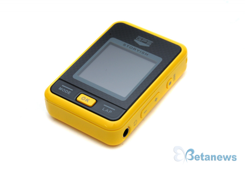
▲ 큐비랩 스토리쉬 포켓GPS(PocketGPS) S1
큐비랩이 출시한 ‘스토리쉬 포켓GPS S1’은 국내 기업으로는 처음으로 순수 개발된 제품으로서, 자전거를 활용한 운동 및 여행은 물론 도보, 등산시 자신의 위치를 인터넷을 통한 지도 서비스를 통해 기록할 수 있는 신개념 레저용 GPS 단말기다.
깜찍하면서도 심플한 디자인에 폭넓은 부가 기능 돋보여

▲ 컴팩트한 사이즈로 휴대성을 높이는 데 일조했다
스토리지 포켓GPS S1은 앞서도 설명했다시피 장시간 자전거를 타고 여행이나 운동을 즐기려는 라이더는 물론, 도보 및 등산시 자신이 위치하고 있는 장소를 구글 어스와 같은 인터넷 지도로 기록해 활용할 수 있는 제품이라고 할 수 있다.
여기에, 얼핏 보면 휴대용 GPS가 아닌 초소형 MP3가 연상될 정도로, 깜찍하면서도 심플한 스타일에 초점을 두고 있다는 것을 쉽게 확인할 수 있다. 또한, 각 모서리의 라운딩 처리와 함께 옐로우 컬러를 채택해 다소 딱딱한 느낌 보다는 산뜻한 분위기를 물씬 풍긴다.
그 뿐만이 아니다. 배터리 4개가 들어간 것과 별반 차이가 없을 정도로 상당히 컴팩트하고 슬림한 사이즈를 부각시켰으며, 무게 또한 휴대폰 보다도 훨씬 가벼운 60g에 불과하기 때문에 잦은 이동에도 뛰어난 휴대성을 보여줄 수 있도록 했다.
특히, 이번 제품은 밤낮을 가리지 않고 휴대하는 사용자를 고려해 OLED(자체발광형 유기물질) 디스플레이를 탑재해 퀄리티를 극대화시키는 데에도 일조하고 있다.
OLED는 일반적인 모바일 기기에 탑재되는 TFT-LCD와는 다르게 자체발광이 가능해 어떠한 환경에서도 밝은 화면을 보여준다는 장점을 가지고 있으며, 실제로 모 대기업의 제품에서 대표적으로 사용되는 디스플레이 방식 중 하나로 수많은 소비자들에게 각광받고 있다.

▲ 초보자도 쉽게 사용할 수 있도록 버튼 구성을 간소화시켰다

▲ 평균속도 및 해발 고도, 나침반 등의 총 5가지 모드를 탑재하고 있다
제품 하단부에는 GPS 및 다양한 부가 기능을 활용할 수 있는 모드(MODE) 버튼을 시작으로, 자신이 이동했던 거리를 단말기로 기록하기 위한 랩(LAP), OK 버튼 등 3가지로 간단하게 구성돼있기 때문에 제품 조작에 미숙한 초보자도 간편하게 사용할 수 있도록 배려했다.
그 중에서도 모드 버튼의 경우 총 5가지로 구성돼 있으며, 기본모드는 1초 간격으로 GPS 로그를 자동적으로 저장해 라이딩 및 도보를 통한 운동, 등산 등에서 활용 가능하며, 운동모드와 고도모드는 구간별 거리 및 시간은 물론 현재 평균속도, 해발 고도를 한눈으로 쉽게 알아볼 수 있다.
특히, 이번 제품에는 고가의 GPS 장비에서만 찾아볼 수 있는 기압 센서를 이용한 고도 측정이 가능하도록 설계돼있다. 이 기능은 제품이 켜진 상태의 위치를 기준으로 고도 그래프를 정밀하게 확인할 수 있다는 장점을 가지고 있어 등산을 즐기는 유저라면 필수적이다.
이밖에, 해당 위치에 대한 위도 및 경도값을 표시하기 위한 나침반 모드는 물론, 현재 수신 중인 위성 정보 및 수신 세기에 따른 위도, 경도를 파악하는 것 또한 가능하다.

▲ 단순 GPS 단말기임에도 불구하고 녹음 및 MP3 재생 등의 다양한 기능을 갖췄다
스토리지 포켓GPS S1은 단순히 제품명으로만 보더라도 GPS 수신기로 생각하는 사용자들이 적지 않을 것이다. 하지만, 이번 제품에는 GPS를 통한 위치 수신 및 이동 거리 측정은 물론, 녹음 및 MP3 플레이어에 이르기까지 다양한 기능을 탑재한 점이 가장 큰 특징이다.
녹음 기능을 활용하기 위해서는 전원이 켜진 상태에서 우측의 위치한 REC 버튼을 길게 3초이상 누르고 있으면 보이스 레코딩 화면으로 전환되면서 쉽게 녹음이 가능하며, 자신이 즐겨드는 MP3 음악을 제품 내부에 탑재된 플래시 메모리로 저장할 수 있다. 참고로 저장 공간은 1.6GB로서 100여개의 MP3 파일을 담아도 전혀 부족함을 느끼지 못한다.
다만, MP3 파일을 넣은 뒤에는 반드시 ‘LP20100228_230001.MP3’와 같이 파일 이름을 변경해야만 정상적으로 재생이 가능하며, 일반 파일명으로는 재생이 불가능하다는 점을 인지하고 있어야 한다. 여기에, 단순 재생만 가능하다는 점도 차후 펌웨어 업데이트를 통해 해결해야할 개선책임에는 틀림없다.

▲ 외장 하드디스크에서 널리 활용되는 미니 USB 인터페이스를 탑재
스토리지 포켓GPS S1의 좌측부에는 PC 연결을 ㎸?미니-USB 포트가 위치하고 있으며, 케이블 연결을 통한 충전이 가능하다. USB 케이블을 통해 완충까지 소요되는 시간은 4시간이며. 최대 휴대할 수 있는 사용시간은 밝기 설정에 따라 최대 11시간까지 가능하다는 것이 큐비랩 관계자의 설명이다.
여기에, 앞서도 설명했다시피 녹음된 파일을 PC로 전송하는 것은 물론 자신의 PC에 저장된 MP3 파일을 내장 메모리로 추가할 수도 있으며, 초보자를 배려한 PDF 규격의 사용 설명서와 함께 GPS 기능을 활용할 수 있는 프로그램이 내장돼있다. GPS 기능 활용에 대한 부분은 다음 페이지에서 알아보도록 하겠다.
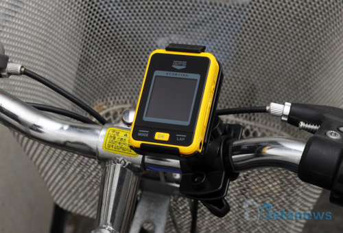
▲ 자전거에 활용하기 위해서는 별도의 자전거 거치대를 구매해야 한다
GPS 로그 기록을 위한 소프트웨어 제공은 기본!

▲ 로케이션 플러스 PC 툴에는 구글 어스가 기본으로 포함돼있다
스토리지 포켓GPS S1은 단순히 제품만으로 모든 기능을 사용하기에는 한계가 있다. GPS 수신을 통한 위치 정보를 지도로 한눈에 확인하는 것은 물론, 자신이 이동했던 장소가 정확하게 어디 지점인지를 파악하기 위한 소프트웨어도 뒷받침되어야 하기 때문이다.
이번 제품에는 이러한 사항을 간편하게 해결할 수 있도록 ‘로케이션 플러스 PC 툴(Location Plus PC Tool)’이라고 불리는 부가 소프트웨어를 기본으로 제공해 단말기 사용에 따른 편의성을 극대화시켰다.
특히, 이 프로그램에는 무료 지도용 소프트웨어로 전세계적으로 명성을 떨치고 있는 구글 어스(Google Earth)맵이 포함돼 있다. 구글 어스에는 포털 서비스 못지 않는 정확한 장소 확인은 물론, 위성을 활용한 스카이뷰, 심지어는 고도 확인까지 한눈에 파악 가능하다.
또한, GPS를 켜고 마지막으로 끈 상태까지의 모든 기록이 남기 때문에, 자신이 이동했던 장소를 별다른 어려움 없이 확인할 수 있다.
물론, GPS 자체가 전파 장비에 약하고 자동차나 특정 건물로 들어갈 경우에는 정상적인 인식이 되지 않는 경우도 발생할 수 있기 때문에, 제품을 손으로 직접 들고다니며 사용하는 것이 좋다. GPS 최초 수신시에는 평균 5초 이내로, 일반 GPS 단말기보다는 빠른 편이다.
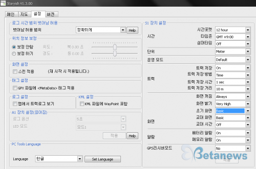
▲ 제품에 대한 장치 설정 및 위치 보정 등이 가능하다
로케이션 플러스 PC 툴의 설정 화면으로 진입하면 GPS 위치 보정은 물론 로그 및 화면, 언어 등이 세부 설정이 가능하며, 장치 설정의 경우 제품에 탑재된 OLED 디스플레이의 화면 밝기 설정과 시간, 트랙, 알람 설정에 이르기까지 다양한 부가 기능이 포함돼있다.
또한, GPS 리시버 기능을 활성화할 경우 별도의 내비게이션을 구입할 필요 없이, 자신의 PC에 설치된 내비게이션 프로그램으로 지도 안내 서비스를 활용할 수 있도록 선택의 폭을 넓힌 것도 이번 제품의 차별화된 장점이다.

◇ 휴대폰에 GPS 기능이 없다면? 큐비랩 스토리시 포켓GPS S1이 대안 = 최근 GPS 기능이 기본 탑재된 최신 휴대폰 및 스마트폰을 시작으로, 다양한 모바일 기기들이 속속 국내 시장에 모습을 드러내고 있다.
하지만, 대부분의 사용자들은 자신의 모바일 기기에 GPS 기능이 있는지 조차도 알 수 없고, 막상 기능이 포함돼있다고 하더라도 제대로 활용하지 않는 경우가 다반사다.
물론, GPS가 우리 생활에 큰 영향을 끼칠 만큼 중요하지 않을 수도 있으나, 여행이나 등산, 자전거를 통한 장거리 이동을 즐기는 유저들이라면 GPS만큼의 필수적인 장비는 찾아보기 힘들 것이다.
이번에 선보인 큐비랩 스토리시 포켓GPS S1은 일반적으로 휴대폰에 내장된 GPS 수신기와 동일하기는 하지만, 평균 속도와 해발고도, 위도 및 경도값을 표시하기 위한 나침반에 이르기까지 다양한 기능을 갖추고 있다는 점에서 상당히 매력적인 제품이라고 할 수 있다.
물론, MP3 플레이어 활용시 재생만 가능하고 GPS 수신시 일부 오류를 일으킨 점이 다소 아쉽기는 하지만, 홈페이지를 통한 지속적인 업데이트로 충분히 개선 가능한데다가 국내 기술로 만들어진 레저용 GPS 중에서는 최초라는 점에서 더욱 의미가 크다.
가격 또한 20만원이상의 턱없는 가격대를 유지하고 있는 일부 외산 제품에 비해, 큐비랩 스토리시 포켓 S1은 10만원대로 비교적 저렴한 데다가 성능 또한 고급형 제품 못지 않는 뛰어난 GPS 수신율를 보여준다는 장점만으로 최상의 메리트를 보여줄 것으로 기대된다.
/ 베타뉴스(http://www.betanews.net)
==========