2015년 3월 12일 목요일


2014년 9월 24일 수요일
Wireless Power Receiver Enables Compact & Efficient Contactless Battery Charging
출처: Electronics technology instruction & product demonstrations videos | EE Times
http://www.eetimes.com/video.asp?section_id=124&doc_id=13209302014년 7월 16일 수요일
3 Phase의 진실을 밝힌다! 메인보드 전원부에 대한 모든것
|
글 : 권용호 / cello@bodnara.co.kr 감수 / 사진 : 장홍식 / potatotree@bodnara.co.kr 들어가면서.. 인텔진영이 시끄럽다. 인텔이 3.06Ghz에서 안정적인 동작을 위해 메인보드 제조사들에게 FMB2에서 70A의 규격을 만족시키는 전원부를 구성하기를 권하면서부터 기존 메인보드들의 전원부 구성에 대한 되새김질이 늘고 있다. 또한 i845PE 메인보드의 전원부 구성에 대한 의구심이 들기 시작하면서 이전까지 그냥 넘어갔던 전원부 구성을 다시한번 돌이켜보게 하고 있다. 또한 이때부터 많이 언급되기 시작한 단어가 바로 'Phase'라는 단어이다. 사실 처음으로 Phase가 제대로 언급되기 시작한것은 Pentium 4 3.06Ghz문제부터가 아니라 Iwill의 XP333 부터라고 해도 과언이 아니다. Iwill XP333은 특이한 구성과 설계로 세간의 관심을 가장 많이 받아온 제품으로, 다른건 모르겠으나 '전원부'하나는 가장 안정적인 AMD메인보드로 손을 꼽았고, 이런 관심을 받아온데 가장 큰 이유가 바로 3 Phase Power Solution 구성때문이다. 이후 수면아래로 가라앉다 다시 Pentium 4 3.06Ghz에서 인텔이 70A 규격을 만족시키는 전원부를 공고한 점, 이후 digitimes에서 이를 '인텔은 4 Phase 구성의 전원부를 권장한다'는 뉘앙스의 글을 포스팅하고 나서부터 전원부 구성과 Phase에 대한 많은 관심이 대두되어 왔다. 또한 현재 내가 사용하고 있는 메인보드는 어떤것이며, 앞으로 구입해야될 메인보드가 어떤 Phase 구성인지가 상당히 대두되고 있는 시점이다. 또하나의 이슈가 있다. i845PE메인보드 대부분이 PCI Clock FIX기능을 지원하면서부터, 오버클럭률에 많은 관심을 보였으며, 'Phase'가 높을 수록 오버클럭이 잘된다는 설이 유포되기 시작하면서 '당연히' Phase 에 대한 관심이 높아졌다. 따라서 우리는 메인보드의 전원부 구성에 대하여 깊이있게 살펴보고, 어떤 결론을 내려야 할지 관심있게 지켜보고자 한다. 사실 이 글은, 앞으로 포스팅 될 'i845PE메인보드 오버클럭 벤치마크'의 앞부분이었으나, 설명이 길고 복잡하여 별도의 칼럼으로 분리하여 포스팅하기로 결정하였다. 따라서 이 글을 읽는분은 앞으로 포스팅 될 오버클럭 벤치마크 기사를 보시는데 많은 도움이 되리라 확신한다.
|
다음을 클릭하시면 이어지는 내용을 계속 보실 수 있습니다. 안정적인 전원부가 10년의 선택을 좌우한다  |
장홍식 기자 / potatotree@bodnara.co.kr
[관련기사]
메인보드 전원부 모스펫 발열 벤치마크 시즌 2, 이번에는 인텔 Z97 메인보드 16종이다

|
보드나라의 기사는 저작자표시-비영리-변경금지 2.0 대한민국 라이선스에 따라 원본 배포처에서 이용할 수 있습니다. Copyright ⓒ 넥스젠리서치(주) 보드나라 원본 배포처 가기 |
2014년 4월 15일 화요일
은근 느린 응답속도의 내 홈페이지
언제부터인가 내 홈페이지의 응답속도가 가끔씩 느려졌다가 (어떤날은 잠깐동안 이나마 접근이 안되는 경우도 있슴.) 정상으로 되돌아 왔다가를 반복하고 있다.
난 손댄거 없는데, 뭐가 문제일까나~???
방문객이 많아서(??) 그런것은 아닐테고, DDoS라면 아예 server가 맛이 갈테니 (내 server 공격해서 얻을게 뭐가 있다고, 설마~~) 그것도 아닌것 같고…
이것 때문에 은근 짜증도 나고 골치도 아프다.ㅠㅠ
2013년 6월 29일 토요일

2013년 6월 20일 목요일
간단하게 만드는 네트워크 에뮬레이터
글쓴이: EzDoum 글쓴날: 2012년 11월 07일 오전 04:55
네트워크 서비스 개발을 해놓고 필드 환경 시험을 해야할 때 다양한 네트워크 상태를 가정하고 테스트를 해봐야 하는데, 네트워크 시뮬레이터 장비로 테스트 하기에는 장비가 너무 비싸서 어렵다.
지난번 tcp 재전송 관련 대학 자료에서 보니까 Netem (traffic control - linux kernel 기능)을 사용해서 packet delay, packet loss, packet duplication, corruption, re-ordering, traffic limit등을 에뮬레이션 할 수 있겠다.
PC or 모바일 - 개발보드(netem) - 개발보드(제품) 으로 망을 구성하면 별도로 비용을 들이지 않고도 테스트 베드 구축 가능함. 개발보드(netem)가 DVR이니까, HDD에 pcap dump도 가능함.
# Netrm
http://www.linuxfoundation.org/print/5212
# TCP Probe (TCP 특정 포트 측정)
http://www.linuxfoundation.org/print/5242
-> Kprobe를 사용해 tcp_recv 함수에서 hook을 등록해서 Congestion windows와 tcp seq num을 추출해서 trace를 남기는 방법임.
-> 즉, Kprobe를 사용하는 예제 쯤 되겠습니다.
http://www.cs.fsu.edu/~baker/devices/lxr/http/source/linux/net/ipv4/tcp_probe.c
# getsockopt(TCP_INFO)
http://linuxgazette.tuwien.ac.at/136/pfeiffer.html
-> tcpprobe는 Kernel 레벨인데 이것은 User level에서 getsockopt로 빼내는 방법임.
Rene Pfeiffer가 쓴 다른 글
http://linuxgazette.tuwien.ac.at/authors/pfeiffer.html
# TC 사용법
http://tcn.hypert.net/tcmanual.pdf
http://www.ezdoum.com/stories.php?story=12/09/23/6714721
# Evaluation of TCP retransmission delays
http://home.ifi.uio.no/paalh/students/EspenSoegaardPaaby.pdf
http://www.ezdoum.com/stories.php?story=12/11/06/1194910
 netem_guide.pdf (352 KiB(360,349 Bytes))
- 출처: http://www.ezdoum.com/stories.php?story=12/11/07/1721190
2013년 5월 26일 일요일

2013년 5월 22일 수요일

2013년 4월 22일 월요일
10 top startups to watch in 2013
Peter Clarke
12/21/2012 2:30 PM EST
Here's our list of ten startups focused on a wide range of electronics technologies that are worth keeping an eye on in 2013.Processors, memory, manufacturing processes, chip architecture, EDA, MEMS, RF, touch screens, servers and the Internet of Things are markets where startups can still make a difference.
What follows are ten rising companies worth tracking in 2013.
Nantero Inc. (Woburn, Mass.) was founded in 2001 and has been working on the use of carbon nanotubes in non-volatile memory applications since then. Having made some noise about a trench-based device structure in 2006 things went quiet again until 2012.
The company has changed its device to an even more scalable in-via structure and has announced additional funding of $10 million led by a couple of strategic partners. In addition microelectronics research center IMEC (Leuven, Belgium) announced a joint development program to make CNT non-volatile memories with critical dimensions of less than 20-nm, and senior IMEC executives expressed the hope that the memory could be deployed as a replacement for DRAM.
If this technology is going to fly it should be able to demonstrate more progress in 2013 and perhaps we will find out who are the strategic partners?
www.nantero.com

Cross-section of Nantero's carbon-nanotube variable-resistence memory structure. The structure is thought to be scalable to 15-nm wide elements and even down to 5-nm.
Related stories:
Partners back nanotube memory for production push
IMEC backs carbon nanotube memories
SuVolta
SuVolta Inc. (Los Gatos, Calif.) was founded as DSM Solutions Inc. in 2005 and originally planned to come to market with a novel form of junction FET. The company went through a reappraisal of its chances and then emerged with CTO Scott Thompson on-board in 2011 touting a fully-depleted planar transistor structure that uses doping to recreate what is done by others with silicon-on-insulator wafers.
Indeed it appeared that PowerShrink transistors with their deeply depleted channel could provide n alternative to FinFET and FD-SOI manufacturing processes, but none of the leading-edge IDMs or foundries appeared to be biting.
That was until Ajit Manocha, CEO of Globalfoundries Inc. (Milpitas, Calif.) said his company was evaluating a third manufacturing process option – besides FinFET and FD-SOI. That option he called super-steep retrograde well (SSRW), which is basically another name for what SuVolta has been doing.
It is not clear whether Globalfoundries is working with SuVolta or independently of them. But either way it helps give SuVolta's technology some credibility and is a good reason to keep an eye on SuVolta in 2013.
SuVolta's PowerShrink transistor manufacturing process achieves FD-SOI-like benefits without requiring SOI wafers as the starting point. It achieves some FinFET benefits with needing to make and protect fins. But will the leading chip companies reject the technology because of NIH?
www.suvolta.com

SuVolta's PowerShrink transistor is deeply-depleted
Related stories:
Globalfoundries mulls third manufacturing option
SuVolta reports 65nm parameter results at IEDM
Tela Innovations
Tela Innovations Inc. (Los Gatos, Calif.) was founded in 2005 and started by working with Qualcomm on computational lithography with a view to the extraction of multi mask information for the double patterning era.
Tela's technology is delivered as physical design representation applied to standard cell logic and embedded SRAM, analog and I/O that can result in area savings and reduced leakage current. The company offers gate-length trade-offs for power, performance and area within its libraries. Tela has also specialized in working with customers' IP development teams to get the technology into production.
In February 2009 Tela acquired Blaze DFM, which added PowerTrim to its technology as well as a relationship with Taiwan Semiconductor Manufacturing Co. Ltd. which bore fruit in 2010.
The company has been fairly quiet since then but did say mid-2012 that it is ready with libraries for the 32/28-nm and 22/20-nm process nodes. The company's investors provide reasons to watch the company. They include: Intel Capital, Cadence Design Systems Inc., KT Venture Group LLC (the investment partner of KLA-Tencor Corp.) and Qualcomm Inc. The fact that the company appointed an intellectual property legal counsel in 2012 is another reason to be watchful.
www.tela-inc.com

Tela offers 28- , 20-nm and FinFET lithography optimized standard cell libraries.
Related stories:
TSMC, Tela trim logic die area by 15 percent
Tela Innovations acquires Blaze DFM
Layout optimization startup Tela buys Blaze DFM
Senseg
Senseg Oy (Espoo, Finland), formed in 2006, has developed a touch interface technology that uses electrostatic field to create the illusion of surface texture and even the movement of keys beneath the fingers. The technology has the potential to provide haptic feedback for touch screens and particularly the on-screen keyboards that are part of the use of smartphones and tablet computers.
The company is backed by Ambient Sound Investments, the investment vehicle of the founders of Skype.
By modulating this attractive force on the fingers a variety of sensations can be generated, including textured surfaces, edges, vibrations and the technology produces tactile sensations with no mechanical vibration. The company appointed a Paul Costigan as CEO in June 2012 and so he should be showing some results from his stewardship of the company in 2013.
www.senseg.com

Use of electrostatics can turn a touch screen into a feel screen
Related stories:
Former Movidius exec joins haptic startup as CEO
Finnish interface developer gets Estonian VC investment
SiTime
SiTime Corp. (Sunnyvale, Calif.), founded in 2005, is a semiconductor company pioneering the use of MEMS timing products.
Earlier this year SiTime entered into a strategic partnership with Vectron International Inc. (Hudson, N.H.) and Knowles Electronics (Itasca Ill.), both owned by Dover Corp. of New York. The formation of the partnership included a cash investment in SiTime by Vectron, which is a maker of quartz timing products, and by Knowles, which makes silicon membrane microphones. The size of the investment was not disclosed but when the competition starts investing in you, you are probably doing something right.
SiTime was also ranked as the fastest growing semiconductor company in North America by Deloitte in November 2012.
www.sitime.com

Silicon MEMS manufacturing brings timing control into the digital domain.
Related stories:
London Calling: MEMS the word
Rusnano draws MEMS firm to Russia
Wilocity
Wilocity Ltd. (Caesarea, Israel), founded in 2007, develops 60-GHz wireless chip sets for the notebook and peripheral markets that can provide data more than ten times faster than today’s wireless LAN solutions. There are numerous competitors but Wilocity appears to have first-mover advantage and announced a number of design wins and partnerships in 2012.
Wilocity's WiGig technology was selected to provide multigigabit wireless connectivity in a Dell Ultrabook featured at the launch of the Windows 8 operating system. Wilocity is also partnered with Marvell Technology Group Ltd. to bring forward tri-band Wi-Fi solutions enabled with 802.11ad for the computing, networking and consumer electronics segments.
www.wilocity.com

Wilocity sits alongside Qualcomm-Atheros on a tri-band board that provides an Ultrabook WiGig solution for Dell Computers.
Related stories:
Four companies prep wave of 60 GHz chips
Wilocity signals next battle at 60-GHz
Cyclos Semiconductor
Cyclos Semiconductor Inc. (Berkeley, Calif.) founded in 2006, announced in 2012 that it was Advanced Micro Devices Inc. that had achieved the first commercial implementation of its resonant clock mesh technology.
It was AMD's Piledriver 64-bit core, which operates at up to and in excess of 4-GHz clock frequency, made using 32-nm bulk CMOS. It was reported to save 24 percent of the power consumption in the clock distribution while achieving previous clock-skew targets.
That leaves upside for the likes of Intel and ARM's partners if they adopt the technology and we would hope to see announcements in 2013.
www.cyclos-semi.com

Schematic diagram of resonant clock mesh technology.
Related stories:
AMD, not ARM, first to use startup's low-power clock IP
Resonant-clocked design tools target ARM core
Adapteva
Andreas Olofsson, CEO of 2008 startup Adapteva Inc. (Lexington, Mass.), has offered innovation in both processor architecture and in funding and business models. To begin with Olofsson managed to make use of multiproject wafer runs to keep costs so low that he was able to boast that he had reached processor IC product release with less than $2 million of total investment, while completing four generations of Adapteva's Epiphany multicore processor.
Then Olofsson went one better and used the Kickstarter crowd-source funding website to raise more than $750,000 for a project to build a personal supercomputer called Parallella for which building blocks would sell at $99. The computer module is based on a combination of Zynq SoCs from Xilinx and an Epiphany processor from Adapteva.
The $750,000 is set to fund a mask set but also has the virtue of seeding a developer community of nearly 5,000 potential customers and a lot of awareness. Of course, being innovative is no guarantee of success but we think these innovations merit keeping an eye on Adapteva in 2013.
www.adapteva.com

Click on image to enlarge.
Adapteva has designed a clean-slate RISC processing engine based on the assumption that electronics is about to enter the manycore era. (Source: Adapteva)
Related stories:
How Kickstarter created a community for Adapteva
Adapteva Kickstarts a $100 supercomputer
Adapteva ships OpenCL compiler for Epiphany
Adapteva close to sampling 28-nm, 64-core coprocessor
Neul
Neul Ltd. (Cambridge, England) was founded in 2010 to develop a wide-area wireless network technology dedicated to machine-to-machine (M2M) communications and the Internet of Things (IoT). The company has pioneered the development of the Weightless standard for networks that operate in the license-free television white space (TVWS) part of the spectrum. Neul's first product is a radio system specifically designed for TV white space that consists of a base station, battery-powered terminal device, antennas and a set of PC-based network management tools.
The founders are experienced in nurturing a startup company, many of them having been founders of Cambridge Silicon Radio in 1998 and in 2012 they got a boost from near neighbors ARM, which added its weight to the Weightless Special Interest Group.
We expect IoT and M2M to be red-hot in 2013 with both Intel and ARM making it an important part of their approach to the market and we also expect Neul to be making news in that sector.
www.neul.com

Neulnet is the first radio system designed to work in the white spaces around TV broadcasts.
Related stories:
ARM joins group driving IoT specs
White space radio startup raises funds
Do machines dream of IoT?
Calxeda
Calxeda Inc. (Austin, Texas), a developer of ARM-based processors and software for low-power servers for data centers, has announced in 2012 that it raised an additional $55 million in equity funding. This puts the total raised by Calxeda over $100 million since the company was founded as Smooth-Stone in 2008.
Calxeda is already shipping the 32-bit EnergyCore processor and with ARM releasing details of 64-bit capable ARMv8 architecture it is expected that Calxeda will continue to make announcements that seek to address a fragmenting server market.
ARM is a significant investor in Calxeda along with: Austin Ventures, Vulcan Capital, Advanced Technology Investment Co. (the owner of Globalfoundries) Battery Ventures, Flybridge Capital Partners and Highland Capital Partners. So expect to Calxeda to be one of the surrogates through which the ARM versus Intel battle is played out in 2013.
www.calxeda.com

Lowering power consumption is at the core of Calxeda's business.
Related stories:
Calxeda roadmap leads to 64-bit CPU in 2014
ARM server platform firm raises big money
Source: http://www.eetimes.com/electronics-news/4403877/10-tech-startups-to-watch-for-in-2013
2013년 3월 22일 금요일
[블루레이] 자이언트 로보: 애니메이션 - 지구가 정지한 날 UE (4disc: 3BD+DVD) 스틸북 한정판
 | [블루레이] 자이언트 로보: 애니메이션 - 지구가 정지한 날 UE (4disc: 3BD+DVD) 스틸북 한정판 -  이마가와 야스히로 감독, 요코야마 미츠테루/미라지엔터테인먼트 - 간만에 강림하신 지름신의 압박이... - 걍 확 사버려~??? - 문제는 내가 Blue-ray player가 없다는거...ㅋㅋㅋ |
2013년 3월 16일 토요일
TI E2E - TPS23754 in flyback mode for 1 Gig POE application
Posted by Arunkumar PB
on Nov 10 2012 02:00 AM
Hi,
We are planning to use TPS23754 in synchronous flyback mode for 1 Gig POE+ application.
In TPS23754EVM-420 ref schematic ,the ethernet interface is not for 1Gig but TPS23754EVM-383 for active clamp forward converter the ethernet interface is for 1Gig.
I want to know if we can use the TPS23754 in synchronous flyback mode for 1 Gig POE+ application.Are there any limitation for TPS23754 in synchronous flyback mode for 1 Gig application.
Please reply
Regards
Posted by Eric Wright
on Nov 12 2012 12:42 PM
Any POE, type 2 equipped ethernet transformer can be used with any TPS23754 based PD (and dc/dc converter topology). You can use the J3 jack from TPS23754EVM-383 with the PD on TPS23754EVM-420 for example. Other POE type 2 giga-bit transformer options are Wurth 749022011 or Pulse H6096NL.
Posted by Arunkumar PB
on Nov 14 2012 00:46 AM
Hi Eric,
Thanks for the reply .So you mean that we can use TPS23754 in fly back topology for 1Gig application only thing that need to be taken care is the TYpe 2 giga- bit transformer.
Posted by Eric Wright
on Nov 14 2012 08:16 AM
Yes, that is correct.
출처: http://e2e.ti.com/support/power_management/power_interface/f/204/t/226086.aspx
on Nov 10 2012 02:00 AM
Hi,
We are planning to use TPS23754 in synchronous flyback mode for 1 Gig POE+ application.
In TPS23754EVM-420 ref schematic ,the ethernet interface is not for 1Gig but TPS23754EVM-383 for active clamp forward converter the ethernet interface is for 1Gig.
I want to know if we can use the TPS23754 in synchronous flyback mode for 1 Gig POE+ application.Are there any limitation for TPS23754 in synchronous flyback mode for 1 Gig application.
Please reply
Regards
Posted by Eric Wright
on Nov 12 2012 12:42 PM
Any POE, type 2 equipped ethernet transformer can be used with any TPS23754 based PD (and dc/dc converter topology). You can use the J3 jack from TPS23754EVM-383 with the PD on TPS23754EVM-420 for example. Other POE type 2 giga-bit transformer options are Wurth 749022011 or Pulse H6096NL.
Posted by Arunkumar PB
on Nov 14 2012 00:46 AM
Hi Eric,
Thanks for the reply .So you mean that we can use TPS23754 in fly back topology for 1Gig application only thing that need to be taken care is the TYpe 2 giga- bit transformer.
Posted by Eric Wright
on Nov 14 2012 08:16 AM
Yes, that is correct.
출처: http://e2e.ti.com/support/power_management/power_interface/f/204/t/226086.aspx
2013년 3월 12일 화요일
2013년 3월 7일 목요일
USB로 노트북 충전과 사용이 동시 가능한 USB Power Delivery 규격은?
하나의 케이블로 자료 교환과 전력 공급이 모두 가능하고, 표준 커넥터를 비롯해 모바일 기기에 맞는 미니 커넥터까지 다양한 규격의 USB는 현재 5Gbps 대역폭의 3.0 규격까지 공개되어 있으며, 이를 이용한 외장하드나 모니터, 웹캠 등 다양한 기기들이 사용되고 있다.
그러나 표준 USB 3.0의 전력 공급 규격은 900mA까지로, 최대 전력 공급량이 4.5W에 불과해 3.5" 외장 하드디스크 구동은 물론 USB 모니터 구동 등 조금만 소비전력이 높아져도 거추장스러운 전원 어댑터가 필요하며, 최신 태블릿과 스마트폰의 대용량 배터리 충전에 오랜 시간이 걸리는 등, USB의 전력 공급 규격의 개선 필요성이 제기되어왔다.
이에 따라 USB-IF에서는 지난 7월 USB 케이블을 이용한 최대 100W 전력 공급 규격인 USB Power Delivery 규격을 확정(이하 PD) 발표, 지난 CES 2013에서 이를 이용한 데모를 시연했는데, 이번 기사에서는 USB PD에 대해 자세히 알아보도록 하겠다.
USB 2.0 이상에 적용 가능한 USB PD
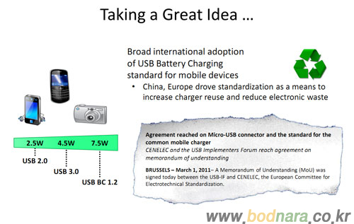
USB PD 규격은 기존 USB 2.0 이상의 규격과 호환을 유지하면서 최대 100W 전력 공급이 가능한 것을 목표로 개발되었기 때문에 기본적으로 USB 3.0은 물론 USB 2.0 이상의 USB 규격에 적용 가능하며, 전력 공급 한계에 따라 총 다섯 가지의 Profile로 구분하고 있다.
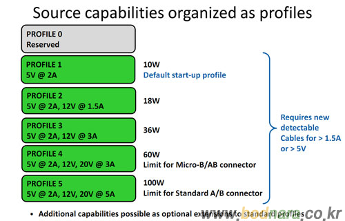
USB PD 규격은 아직 확정되지 않은 Profile0을 비롯해 10W 규격의 Profile1부터 18W 규격의 Profile2, 36W 규격의 Profile3, 60W 규격의 Profile4, 100W 규격의 Profile5로 구분되며, 60W의 Profile4는 마이크로 B/AB 커넥터, 100W의 Profile5 규격은 스탠다드 A/B 커넥터를 사용하도록 규정하고 있다.
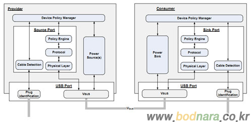
USB PD는 케이블과 장치를 감지해 전력을 자동 조절한다
기존 5V@900mA에 머물던 USB 3.0의 경우 전력 공급 능력이 최대 22배, 5V@500mA였던 USB 2.0의 경우 40배 이상 확대되므로, 안전을 위해 USB PD 규격에서는 케이블의 PD Profile 지원 마커를 포함해 재디자인된 전용 케이블 사용을 권하고 있으며, 케이블 규격을 감지해 공급 가능한 최대 전력을 자동 조절한다.
PD 규격을 위해 변경된 커넥터 구조
USB PD 규격은 기존 규격과의 호환을 유지하면서 전원 공급 능력을 강화한 규격으로 기존 USB 2.0과 USB 3.0 스펙에서 크게 변한 부분은 없이 기존 USB 커넥터/ 플러그 규격에서 전원 공급과 데이터 교환을 위해 사용되었던 기본적인 핀 구조를 그대로 활용하기 때문에 외형적으로 사용자가 체감할 수 있는 변화는 크지 않다.
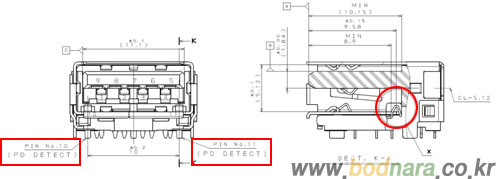
USB 3.0 PD 스탠다드 A 커넥터
USB PD 스탠다드 A 플러그(좌) / USB 스탠다드 A 플러그
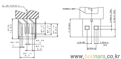
USB PD 규격의 커넥터/ 플러그 규격은 기존 USB와 기본적인 규격은 거의 변경된 점이 없지만, 기존 USB 규격과 PD 규격을 구분하기 위해 커넥터에 감지 핀이 추가되고 플러그의 디자인이 소폭 변경되었다.
즉, PD 스탠다드 A형의 경우 기존 스탠다드 A형과 비교해 PD 케이블 감지와 플러그 삽입 상태를 확인하기 위한 핀이 추가되었으며, 플러그는 커넥터 내부에 PD 감지 핀과의 접촉을 위해 플러그의 금속재 하우징이 약 1mm 가량 길어졌다.
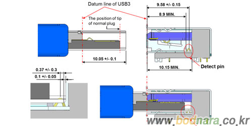
이와 같은 구조 변경을 통해 PD 스탠다드 A 커넥터는 감지 핀을 통해 연결된 해당 플러그(케이블)가 PD 규격을 지원하는지 확인하고, 케이블 내 마커에 기록된 규격에 맞춰 최대 공급 전력을 조절한다.
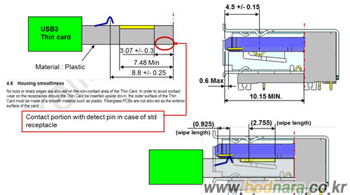
한편, 기존 USB 플러그는 USB PD 커넥터 내의 감지 핀과 접촉하지 않으므로 표준 USB 규격에 따라 전력을 공급(USB 2.0 : 5V@500mA, USB 3.0 : 5V@900mA)하며, 일부 씬 카드의 경우 감지 핀과 접촉되는 플러그 부분을 비전도성 물질로 제조해 잘못된 전력 공급이 이뤄지지 않도록 할 것을 규정하고 있다.
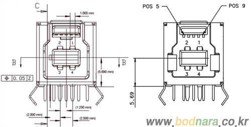
USB 3.0 PD 스탠다드 B 커넥터(좌)/ USB 3.0 스탠다드 B 커넥터(우)
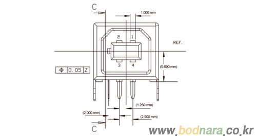
USB 3.0 PD 스탠다드 B 타입의 경우 기존 Powered-B 커넥터와 동일한 구성으로, 커넥터 중앙 좌측에 플러그 감지를 위한 추가 핀과 플러그 삽입 상태 확인을 위한 핀이 추가되었다.
USB 2.0 PD 스탠다드 B 커넥터
USB 2.0 PD 스탠다드 B 커넥터의 경우 기본적으로 USB 3.0 PD 스탠다드 B 커넥터에서 USB 3.0을 위해 추가된 부분을 제거한 형태로, PD 규격 케이블 감지를 위한 핀이 중앙 좌측에 추가되었다.
커넥터와 플러그가 기존 버전과 호환성을 유지한 채 PD 규격 케이블 감지를 위한 구조가 추가된 만큼 케이블 역시 해당 케이블이 지원하는 PD Profile 감지 기능을 제공하도록 요구하고 있으며, 안전을 위해 처음에는 표준 USB 규격으로 동작해 PD Profile을 감지한 후 해당 PD Profile 규격에 따라 동작하는 방식을 취하고 있다.
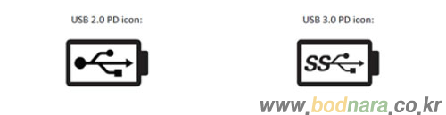
한편, USB PD 규격은 USB 2.0과 USB 3.0을 모두 지원하므로 각각의 아이콘으로 구별하고 있는데, 기본적으로 해당 USB 규격의 표준 아이콘과 배터리를 뜻하는 아이콘을 결합해 구분하고 있다.
호환성을 유지하며 발전해가는 USB
현재 5Gbps 대역폭의 3.0 규격까지 발전한 USB 규격은 지난 2012년 7월 USB 기기의 최대 전력 공급 능력을 100W까지 늘린 Power Delivery 규격이 제정되고, CES 2013에서 제품 시연이 이뤄졌다.
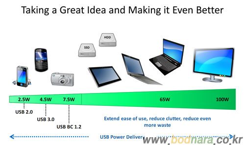
USB PD는 USB 케이블만으로 최대 100W의 전력을 공급할 수 있기에 그동안 별도의 전원 어댑터가 필요했던 USB 외장 기기들을 USB 케이블만으로 활용할 수 있어, 위 시연 영상과 같이 고정식으로 이용하는 중앙 모니터를 전원 소스로 활용해 노트북을 활용하는 것도 가능하다.
USB가 하위 호환을 유지하면서 발전해온 것 처럼 이번 PD 규격 역시 기존 규격과 호환되지만, PD 규격을 제대로 활용하기 위해서는 이에 맞는 기기와 케이블이 필요하기에 추가 지출이 필요하며, 지난 CES 2013에서 첫 시연을 가진 만큼 실제 적용된 제품을 만나기에는 상당한 시일이 필요할 것으로 보인다.
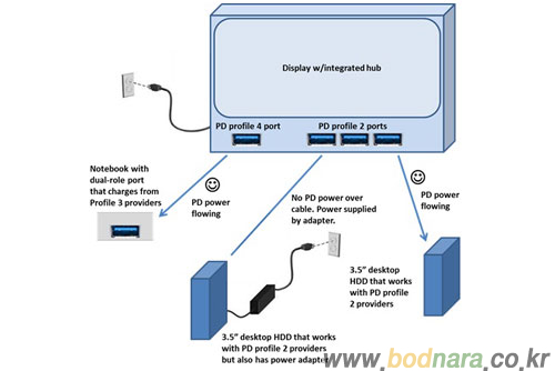
아직 상용화 제품도 선보이지 않은 규격이기에 앞으로를 점치긴 조심스럽지만, 최소한 3.5" 외장 하드디스크 구동이 가능한 Profile2까지는 비교적 빠르게 보급될 것으로 전망되며, 이동이 잦은 비즈니스용 노트북이나 다수의 USB 장치를 사용하는 데스크탑 환경에서 일정 수요가 있을 것으로 예상된다.
한편, USB-IF에서는 현재 PD 규격 이후 5Gbps인 USBs 3.0의 대역폭을 2배로 늘리기 위한 작업을 진행 중으로, 분명히 USB가 현 시점의 PC 시장에서 가장 보편적인 외장형 인터페이스임에는 분명하지만 보다 높은 성능과 기능으로 추격해오는 타 인터페이스와의 경쟁에서 살아남기 위해 노력하는 모습을 보이는데, 다음에는 어떤 곳에서 변화하는 모습을 보여줄지 기대된다.
이상호 기자 / ghostlee@bodnara.co.kr
[관련기사]
SSD를 활용하는 또 다른 방법, 외장 저장장치로의 변화
성질급한 한국인을 위한 충전 기술, 기가바이트 ON/ OFF Charge
차세대 USB 3.0은 기대에 부응할 수 있을까?
USB 3.0 시대에 어울리는 스마트하드, LG 스마트하드 XE2!!
USB 3.0+7200RPM HDD+클라우드 백업, 히타치 TOURO Mobile Pro
| |
보드나라의 기사는 저작자표시-비영리-변경금지 2.0 대한민국 라이선스에 따라 원본 배포처에서 이용할 수 있습니다. Copyright ⓒ 넥스젠리서치(주) 보드나라 원본 배포처 가기 |
2013년 2월 27일 수요일
TI E2E - Re: TPS2065CDBVR Wave Soldering Profile
TI E2E - Re: TPS2065CDBVR Wave Soldering Profile
TPS2065CDBVR Wave Soldering Profile
========== QUESTION ==========
Posted by Ivy Ong
on Feb 22 2012 03:16 AM
Hi,
Can you share with me the Wave/Flow Soldering Profile for TPS2065CDBVR (SOT23).
Or is there any link that I can download the profile from?
Thanks
========== ANSWER ==========
Posted by Martin Patoka
on Feb 23 2012 07:42 AM
The DBV package is qualified for reflow according J-STD-020 standard for maximum 260°C reflow temperature on the package, with a slow preheating to this temperature. Commonly a full convection reflow oven is used for this process.
Using the TPS2065CDBVR in a wave solder process (bottom-side mounted, and immersed in solder wave) is not qualified by TI and is at the customer's risk. The reason is that the package sees a thermal shock when the board moves from the preheating stage (around 150-180°C) into the liquid solder wave which may exceed 260°C for leadfree soldering. A part mounted to the topside (not in the solder) during wave will be OK with normal process temperatures..
There is not a specific profile recommended if the part is subjected to wave soldering. It usually is dependent on the equipment settings and structure. The solder and flux suppliers involved in that process may have general recommendations.
For reflow soldering, using SnAgCu leadfree solder pastes, the solder paste supplier recommendation is the first step to consider. Usually the peak temperature for reflow soldering is somewhere in the 235-245°C range to form the solder joint. This depends on the variations of packages on the board. Small packages may get hotter than larger ones during the reflow pass.
TPS2065CDBVR Wave Soldering Profile
========== QUESTION ==========
Posted by Ivy Ong
on Feb 22 2012 03:16 AM
Hi,
Can you share with me the Wave/Flow Soldering Profile for TPS2065CDBVR (SOT23).
Or is there any link that I can download the profile from?
Thanks
========== ANSWER ==========
Posted by Martin Patoka
on Feb 23 2012 07:42 AM
The DBV package is qualified for reflow according J-STD-020 standard for maximum 260°C reflow temperature on the package, with a slow preheating to this temperature. Commonly a full convection reflow oven is used for this process.
Using the TPS2065CDBVR in a wave solder process (bottom-side mounted, and immersed in solder wave) is not qualified by TI and is at the customer's risk. The reason is that the package sees a thermal shock when the board moves from the preheating stage (around 150-180°C) into the liquid solder wave which may exceed 260°C for leadfree soldering. A part mounted to the topside (not in the solder) during wave will be OK with normal process temperatures..
There is not a specific profile recommended if the part is subjected to wave soldering. It usually is dependent on the equipment settings and structure. The solder and flux suppliers involved in that process may have general recommendations.
For reflow soldering, using SnAgCu leadfree solder pastes, the solder paste supplier recommendation is the first step to consider. Usually the peak temperature for reflow soldering is somewhere in the 235-245°C range to form the solder joint. This depends on the variations of packages on the board. Small packages may get hotter than larger ones during the reflow pass.
TI E2E - RE: Manufacturing process
TI E2E - RE: Manufacturing process
========== Question ==========
Posted by Satyaprakash R1
I have query regarding manufacturing process for few parts.
1. Please let me know the reflow parameters specification or do you follow the J-STD-020 standard or any other standard.
2. What kind of reflow solder process is allowed? ( for example Hot Air/Convection, IR , Vapor Phase, )
3. Is wave soldering is allowed for these parts?
4. What kind of flux is used for example rosin, resin, Organic, Inorganic etc,
5. What kind of rework is preferred for example hand, Hot air, etc and its peak temperature.
6. We would also like to know the recommended method for cleaning. For example Water, Alcohol any other
If you any proper document for manufacturing/Assembly process please provide me that.
Here by I am attaching spread sheet where choices for each fields are noted in comments.
========== Answer ==========
Posted by JohnTucker
In general we follow J-STD-020. The maximum allowed reflow temperature is stated on the Moisture Sensitivity Label (MSL).
========== Question ==========
Posted by Satyaprakash R1
I have query regarding manufacturing process for few parts.
| TPS61170DRVR |
| CLVC1G125MDCKREP |
| CD74HC125QPWRQ1 |
| SN74AHC1G04QDBVRQ1 |
1. Please let me know the reflow parameters specification or do you follow the J-STD-020 standard or any other standard.
2. What kind of reflow solder process is allowed? ( for example Hot Air/Convection, IR , Vapor Phase, )
3. Is wave soldering is allowed for these parts?
4. What kind of flux is used for example rosin, resin, Organic, Inorganic etc,
5. What kind of rework is preferred for example hand, Hot air, etc and its peak temperature.
6. We would also like to know the recommended method for cleaning. For example Water, Alcohol any other
If you any proper document for manufacturing/Assembly process please provide me that.
Here by I am attaching spread sheet where choices for each fields are noted in comments.
========== Answer ==========
Posted by JohnTucker
In general we follow J-STD-020. The maximum allowed reflow temperature is stated on the Moisture Sensitivity Label (MSL).
John Tucker
Consumer DC/DC Applications
Consumer DC/DC Applications
2013년 2월 6일 수요일


2013년 1월 2일 수요일
PMIC 시장 쏠림 현상 심화…국내 업계 자생력 조기에 키워야
[ 2013년 01월 01일 ]
고부가가치 반도체로 각광받는 전력관리반도체(PMIC) 시장에서 외국계 선두 업체들의 쏠림 현상이 심화되고 있다. 중저가 시장에서는 대규모 양산 능력을 갖춘 일부 업체가 가격 경쟁을 주도하고 있고, 스마트폰용 고부가 PMIC 시장도 선두 업체가 싹쓸이하는 추세다. 삼성전자·실리콘마이터스·실리콘웍스 등 국내 PMIC 업체들이 서둘러 자생력을 확보해야 한다는 목소리다.
1일 업계에 따르면 최근 TI·맥심 등 외국계 PMIC 선두 업체들은 성능과 가격 경쟁력을 앞세워 시장을 독식하고 있다.
우선 중저가 PMIC 시장에서는 가격 경쟁 양상이 수위를 넘어섰다. 근래 중저가 모바일용 PMIC와 LCD 디스플레이·백라이트유닛(BLU) 구동용 PMIC는 가격이 40~70센트까지 떨어졌다. 가격 하락은 TI가 주도했다. TI는 지난해부터 200mm(8인치) 웨이퍼 생산 공정(팹)을 300mm(12인치) 공정으로 전환했다. 웨이퍼 크기를 키우면서 생산 원가를 대폭 낮췄다. 자체 팹을 이용해 설계 기간도 단축했다. 맥심 역시 지난 2010년부터 300mm 팹에서 PMIC를 양산했다. 실리콘마이터스 등 국내 업체는 여전히 200mm 웨이퍼 팹을 이용하고 있다. 동부하이텍과 하이닉스는 아직까지 300mm 웨이퍼 팹 생산 계획이 없다. 삼성전자를 제외하면 자체 팹이 없어 설계 후 테스트·양산까지 기간이 오래 걸린다는 것도 걸림돌이다.
세계 모바일 시장이 삼성전자와 애플의 양강 구도로 고착화된 것도 가격 인하를 부추기고 있다. 업계 관계자는 “성능과 가격에 대한 양사의 요구 수준이 한층 높아진 데다 TI가 저가격 정책을 쓰면서 거의 치킨게임 양상이 벌어지고 있다”고 말했다.
반면 프리미엄 스마트폰 등에 공급되는 고성능 PMIC는 국내 업체들이 넘볼 수 없는 영역이다. 모바일용 고성능 PMIC 시장을 석권한 맥심인티그레이티드가 타의 추종을 불허하는 이익을 내는 이유다. 갤럭시S3 등 프리미엄 스마트폰용 PMIC는 현재 1달러를 훌쩍 넘는 가격에 거래된다. 이에 따라 맥심은 올해(6월 결산 기준) 영업 이익률이 22.25%에 육박했다. 국내 PMIC 업체 실리콘마이터스는(작년 말 기준) 13%에 불과했다. 올해는 영업 이익률이 이보다 더 떨어질 전망이다.
조규형 KAIST 전자공학과 교수는 “스위칭파워와 극저잡음(LDO) 레귤레이터를 10개 이상 집적하면 간섭·노이즈 현상이 발생하기 때문에 고성능 PMIC는 높은 기술력이 필요하다”며 “국내 업계의 시장 진입이 늦었던 탓에 앞으로도 상당기간 기술과 노하우를 축적해야 할 것”이라고 말했다.
오은지기자 onz@etnews.com
출처: 전자신문 (http://www.etnews.com/news/device/device/2699666_1479.html)
2012년 11월 22일 목요일
PLDWorld server is On-Line again~!!!
지난 9/27 고장났던 기존 PLDWorld server는 버리고, 이번에 중고 server를 하나 장만해서 다시 가동을 시작했습니다...
OS설치하고, application 설치하고, backup 자료 복사하고, 등등등...
간만에 복구작업 진행하려니 힘도들고 귀찮아서 update도 거의 안하는 마당에 아예 운영을 관둘까 했습니다만, 그동안 운영했던게 아까워서 그냥 하기로 맘먹고 복구작업 진행을 했습니다...
많은 어려움이 있었습니다만, 지금은 다시 정상상태로 복귀되어 정상적인 service를 진행하고 있습니다...^^
OS설치하고, application 설치하고, backup 자료 복사하고, 등등등...
간만에 복구작업 진행하려니 힘도들고 귀찮아서 update도 거의 안하는 마당에 아예 운영을 관둘까 했습니다만, 그동안 운영했던게 아까워서 그냥 하기로 맘먹고 복구작업 진행을 했습니다...
많은 어려움이 있었습니다만, 지금은 다시 정상상태로 복귀되어 정상적인 service를 진행하고 있습니다...^^
2012년 9월 28일 금요일
제품 안 이모저모: 구글 ‘넥서스7’

디스플레이/광전자
게재:2012년09월28일
Allan Yogasingam
EE Times
아마존은 작년에 최초의 200 달러 미만 태블릿인 '킨들 파이어'를 선보이며 가전 시장을 뒤흔들어 놓았다. 많은 이들이 이 온라인 업체의 전자 시장 진입에 대해 회의적이었지만, 일부에선 이를 천재적인 일격으로 보았다. 아마존은 자신들이 보유하고 있는 방대한 온라인 타이틀 자산을 이용해 업계 리더인 애플과 콘텐츠 면에서 경쟁할 수 있는 위치에 올라섰다.
'킨들 파이어'는 e북, 음악 및 영화를 망라하는 아마존의 라이브러리와 최저 가격대의 태블릿을 결합함으로써 즉각적인 히트 제품이 되었다. 2011년 4사분기에는 600만 대가 넘는 '킨들 파이어'가 판매되어 아마존은 전체 시장의 16.8 퍼센트를 차지하며 세계 제2위의 태블릿 제조업체로 올라섰다고 IDC는 밝혔다.
그런데도 아마존의 모델을 따라 하려는 업체들이 별로 없었다는 것은 이상한 일이었다. 태블릿 제조업체들은 아직도 애플과 경쟁하려 하고 있으며, 아이패드에 가깝거나 보다 나은 사양의 제품들을 내놓고 있다. 덕분에 400 달러 이하의 태블릿은 별로 없는 형편이다.
아마도 '킨들 파이어'에 대적할 수 있는 태블릿을 제공할 만한 자원과 콘텐츠를 보유하고 있는 업체는 구글 하나뿐일 듯싶다.
최초의 구글 브랜드 핸드폰인 '구글 넥서스 원(Google Nexus One)'은 HTC에 의해 제조되었으며, 구글이 소비자들에게 직접 판매한 최초의 핸드폰이기도 하다. 이 제품은 '넥서스 S', '넥서스 원' 및 '갤럭시 넥서스(Galaxy Nexus)'와 같은 다른 구글 장치들을 위한 템플릿 역할도 했다. 매번 제품을 내놓을 때마다 구글은 저명한 장치 제조업체와 협력관계를 맺는 한편으로 자신들은 사용자 인터페이스에 노력을 집중하고 특정 장치를 위한 안드로이드 운영체제를 최적화했다.
그리고 마침내 구글은 자사 최초의 브랜드 태블릿인 '넥서스7(Nexus 7)'을 지난 6월 27일에 개최된 I/O 컨퍼런스에서 선보였다. '넥서스7'의 가격은 199 달러로서, 이는 '킨들 파이어'와 직접 경쟁하게 될 것임을 뜻한다. 안드로이드 OS, 그 중에도 특히 '허니콤(Honeycomb)'은 아이패드의 경쟁자들에 의해 오래 전부터 사용되어 왔다. '넥서스7' 태블릿에는 안드로이드의 최신 4.1 버전인 '젤리빈(Jelly Bean)'도 포함되어 있다.

그림 1. 구글 '넥서스7'은 199 달러에 불과하며 풍부한 어플리케이션 라이브러리를 갖추고 있다.
'킨들 파이어'처럼 '넥서스7'은 다른 태블릿에 견줄만한 사양을 제공할 뿐만 아니라 구글 안드로이드 마켓을 통해 구입 가능한 풍부한 어플리케이션 라이브러리를 갖고 있다. 또한 7인치 디스플레이를 탑재한 '넥서스7'은 엔비디어의 쿼드코어 프로세서 '테그라3'와 1 GB RAM을 내장하고 있으며, 최대 16 Gb의 저장공간을 옵션으로 제공한다.
내부에는 무엇이?
'테그라3' 프로세서는 ASUS Transformer Prime 내부에 처음으로 사용된 이래로 꾸준히 그 채택이 늘어왔다. 우리의 IRIS 데이터베이스에 따르면, '테그라3'는 새로운 마이크로소프트 서피스(Surface) 태블릿에 사용된 것을 비롯해 최소한 다섯 개의 디자인 윈을 달성했다.
이 1.3 GHz의 저전력 SoC는 CPU와 GPU에 각각 네 개의 코어를 포함하는 최초의 모바일 어플리케이션 프로세서였다. '테그라3'는 "가변 대칭 멀티프로세싱" 기능을 갖는데, 이것은 전력소모가 덜한 작업에 저전력의 단일 코어를 사용한다.

그림 2. '넥서스7'의 통신 보드 앞면
새로운 벤더들
'넥서스7'의 칩 공급업체들 가운데는 주요 전력관리 IC(MAX77612A)를 제공하는 맥심(Maxim)사와 같은 친숙한 업체들도 있으며, 텍사스 인스트루먼츠(TI)사의 디자인 윈 두 개도 전력관리와 관련이 있다. 우리는 샌디스크/도시바(SanDisk/Toshiba)사에서 제조한 Kingston사의 8Gb 메모리 모듈과 NXP사의 PN65 NFC 보안 모듈도 발견했다. 후자의 경우, 최근 삼성 '갤럭시S3'에서도 찾아볼 수 있었다.
브로드컴(Broadcom)사의 블루투스 무선 트랜시버용 BCM4330 802.11n과 BCM4751 통합 GPS 수신기가 채택된 것도 주목할 만하다. BCM4330은 AzureWave AW-NH665 802.11n 와이파이/블루투스/FM 무선 모듈과 짝지어져 있다.
태블릿에서는 보통 볼 수 없는 칩 제조업체들 가운데 하나인 ELAN Microelectronics사는 '넥서스7'의 터치스크린용 컨트롤러를 제공했다. 전에는 이 회사의 마이크로컨트롤러가 중국 시장용으로 제조된 핸드폰에 사용된 것을 본 적이 있는데, '넥서스7'은 이 대만 벤더에게 있어서 중요한 디자인 윈인 셈이다.
하이엔드 프로세서와 안드로이드 4.1 젤리빈(Jelly Bean)용으로 최적화된 다수의 어플리케이션들 그리고 8Gb 모델의 경우 199 달러라는 가격의 조합은 구글에게 태블릿 시장에 영향을 미칠 수 있는 기회를 주고 있다. 초기 징후들로 봐서는 '넥서스7'의 선주문은 상당해 보인다. 구글이 '넥서스7'에서 성공을 거둔다면 애플도 7인치 모델을 내놓아야 한다는 압박이 커질 것이다. 이를 싫어한 고 스티브 잡스의 뜻에도 불구하고 말이다.
주요 부품들:
· 엔비디아 테그라3: 쿼드코어 모바일 어플리케이션 프로세서
· 하이닉스 H5TC2G83CFR: 2 Gb DDR3 SDRAM
· Kingston KE44B026BN: 8GB 메모리 모듈
· Realtek (RMC) ALC5642: 오디오 코덱 및 헤드폰 앰프
· 맥심 MAX77612A: 전력관리 IC
· 텍사스 인스트루먼츠 TPS63020: 벅-부스트 컨버터; SN75LVDS83B LVDS 디스플레이 Serdes
· 페어차일드 FDMC6675BZ: P 채널 파워 MOSFET
· ELAN Microelectronics eKTF3624BWS 및 eKTH1036BWS: 저항성 터치스크린용 컨트롤러
· Broadcom BCM4751: 통합 모놀리식 GPS 수신기
· InvenSense MPU-6050: 6축 (자이로 및 가속도계) MEMS 디바이스
· AzureWave AW-NH665: 802.11n 와이파이/블루투스/FM 무선 모듈
· NXP반도체 PN65: 보안 NFC 모듈

그림 3. '넥서스7'의 통신 보드 뒷면
출처: http://www.eetkorea.com/ART_8800675374_480703_NT_5713f945.HTM
좀 더 선명하고 자세한 사진들이 필요하시면 본 기사의 원문이 실려있는 http://www.eetimes.com/electronics-news/4376737/Teardown--Google-s-Nexus-7-를 방문하세요…
피드 구독하기:
글 (Atom)