2006년 6월 2일 금요일

Power Management DesignLine | How you can manage multiple voltages in portables

03/23, 2005

How you can manage multiple voltages in portables


The proliferation of low-voltage processor, DSP and FPGA applications has created a need for digitally programmable power management control functions to meet the increasingly stringent supply rail requirements and the rapid changes placed on the power chain. Since system supply requirements change rapidly, a new "platform solution" that can change to meet any type of system power supply requirement eases the designer's job. This can be achieved by specifying a power "block" that can be standardized over a wide variety of applications and then digitally configured to individual requirements.

Typically, DC-DC converters are specified to meet ±2% initial setpoint accuracy and 3% over input voltage, loading and temperature conditions until end of life. This is insufficient for performance, testing and reliability reasons. Device voltage levels for multi-voltage Processors, DSPs and ASICs have fallen to 0.9V and are approaching 0.6V, making system voltage tolerances tighter and necessitating a new way to keep these voltage levels within specifications. If these requirements are not followed, performance degradation, fault conditions such as bus contention or device latch-up can arise. This article describes the importance of accurate DC output voltage control and a method to actively control any standard adjustable DC-DC converter module, discrete DC-DC PWM controller or LDO over time and temperature. A reference design using a standard Point-of-load (POL) DC-DC converter footprint and discrete switching regulator is shown with extremely accurate ±0.2% output levels. The POL automatically adjusts supply output voltage levels under all DC load conditions with programmable supply voltage margining allowing in-system test and control. A programmable 9-channel power supply PWM controller design is shown exhibiting ±0.5% accuracy. It forms a complete portable power system under digital control allowing dynamic adjustment of output voltage levels.

The need for accuracy and programmability As processor supply levels drop, both input current and voltage accuracy requirements increase. For this reason, systems are migrating from isolated distributed power to non-isolated distributed power architectures using POL solutions to gain improved voltage regulation and control at the load (Figure 1). Isolated distributed power uses 2 or more -48V isolated step-down DC-DC converters, which then route separate lower voltage supplies across the board. In the point of load distributed architecture, the -48V powers a single isolated DC-DC converter to provide an intermediate bus voltage. This intermediate bus voltage then powers many non-isolated DC-DC converters or LDO's at the load as shown in Figure 1.

Necessary power management functions

Figure 1 -- An example card design with power management functions necessary in data communications systems. These functions include Hot Swap, Supply Cascading/Sequencing and Tracking, Environmental Monitoring and Reset Control. As component power requirements change, the power management device can be in-system programmed using the I2C bus. The power supply is bussed from a main power bus and down converted directly at the load.

This architecture is more desirable because components making up the heart of the line card require lower voltages and higher currents and regulating at the load reduces inaccuracies. Power Management controllers are included to turn on/off and continuously monitor the POL supplies. Providing power at the load gives superior regulation, transient response and avoids voltage drops across PCB traces. This is necessary because as voltage levels decrease, allowable supply variations around these levels also decrease. Devices now not only require specific power supply turn on sequencing, but they also run at 1V or lower levels. These tighter limits demand more accurate control especially under changing load conditions and temperature variations to maintain optimal performance. The power system must automatically adjust and also test the limits of each board to guarantee performance and reliability. A highly integrated and accurate power supply manager, monitor and sequencer can achieve this required performance.

Processors are being marketed with various operating frequencies. For example, a processor with an operating frequency of 300MHz and a processor from the same manufacturer with an operating frequency of 700MHz are not fundamentally different. In fact, the 300MHz processor is not designed to run at 300MHz, it simply failed to perform to specification at 700MHz. Any processor manufacturer's data sheet will show that the higher performing processors are the result of processors yielding over a more stringent power supply rating.

The tighter power supply tolerances dictated by the high performance processor manufacturers have placed a heavy burden on the system designer. Typically, a processor's power supply tolerance is ±2.5%, which is ±25mV for a 1V supply. This power supply tolerance needs to be maintained over the full operating temperature of the board. When these challenges are compounded with board layout issues such as voltage drops across the power traces, board designers can find themselves in a desperate situation with a looming deadline.

There are several factors that affect the accuracy of a power supply. Take for example the standard structure of the non-isolated DC-DC converter shown in Figure 2. The resistor divider created by R1 and R2 sets the output voltage of the converter by feedback to the error amplifier against the reference voltage. This feedback keeps the inverting input terminal of the error amplifier and therefore the output of the supply equal to the converter's reference voltage. Inaccuracies in resistors R1 and R2 will cause errors in the set point of the converters output voltage. Variations in these resistors over temperature will increase the cumulative error. Errors in the converter's reference voltage also causes inaccuracy of the output voltage. Board layout can also decrease the accuracy of the DC-DC converter. Improper placement of the converter's voltage sense lines can result in uncompensated power trace IR losses to the load point.

Active DC Output Control
Active DC Output Control (ADOCTM) is one method of accurately controlling the output of a DC-DC converter or LDO to achieve high accuracy power supply voltages. Active DC Output Control is a new approach to intelligent power management. Using ADOC a designer can control the output of DC-DC converters or LDOs to ±0.2% for applications involving high performance processors. ADOC controls the output of a converter by effectively adjusting the resistors that set the output voltage of either a DC-DC converter or adjustable LDO. An ADOC solution is typically connected to a DC-DC converter as shown in Figure 2. The ADOC circuit stores the desired output voltage as a digital 10-bit value in non-volatile memory. The ADOC circuitry monitors the converters output at the load. After significant filtering and signal conditioning, the converter's output is compared to an inexpensive reference voltage accurate to ±0.1%. A decision is then made to increase or decrease the control signal to adjust the converter's output to the desired voltage ±0.2%.

ADOC connection

Figure 2 " The ADOC connection to a standard DC-DC converter. The ADOC function Controls DC-DC Converters via the TRIM pin. The CTRIM_CAP and RTRIM component type and values are determined for optimal operation. The RTRIM resistor is not necessary for DC-DC converter modules employing an on-board Trim Resistor.

The Output voltage in Figure 2 is derived from the following equations:
Eq1...Equation 1

Eq2...Equation 2

Where: 0.3 = TRIM output saturation voltage
Equation 3

and Vnom = Nominal non-trimmed output voltage

One problem with attempting to control the output voltage of a power supply is the possibility of interfering with the power supply's feedback control loop. Using two control loops is inherently risky and sometimes results in system instability. ADOC, however, uses a system of nonlinear, inherently convergent control to maintain system stability when coupled with the converter's control loop. The control loop of a DC-DC converter is optimized for fast transient response. On the other hand, the goal of ADOC is to accurately control the DC or average level of the output voltage. For controlling the DC voltage level the ADOC control loop runs very slow at 500Hz whereas the converters control loop responds to frequencies in the tens to hundreds of kHz. This large separation of loop response alone however does not guarantee system stability. The ADOC control loop employs a nonlinear digital control element where the adjustment to the output is always of the same magnitude. This nonlinear control induces a very small ripple voltage on the converter's output voltage. For any noise in the system with a magnitude greater than this induced ripple the gain of the ADOC control loop is less than 1. For noise of magnitude less than the induced ripple the gain is greater than 1. This noise is amplified until its magnitude is greater than the induced ripple where the loop then has a gain of less than 1. This sequence is referred to as a stable limit cycle in nonlinear systems. The induced ripple can be set with the ADOC circuit to less than 100μVp-p thus rendering it negligible.

The ADOC circuit is superior to simply using higher accuracy components such as the feedback resistors and the voltage reference for several reasons. The ADOC circuit actively controls the power supply's output so changes in temperature that affect the components of the converter result in only the ultra-low temperature variation associated with the ADOC circuit itself. Also, through the use of non-volatile memory to set the output voltage, ADOC can be used to voltage margin a converter's output accurately. This margining is a common practice among board designers to determine the robustness of a design by subjecting the board to the various voltage ranges. Some products use voltage margining as a production test to ensure system reliability. A returned board from the field is costly. Given this, companies are fearful of having marginal components on their boards. This has resulted in mandates for voltage margin testing every board that is manufactured.

The mechanism of supply margining is the same as that of supply controlling: adjust and hold the DC value of the supply. So naturally, ADOC also benefits voltage margin testing. If a mandate is set to margin test boards to ±10% with supplies that are only accurate to ±4%, the results can be unpredictable. For instance, are the supplies being margined to ±6% or are they margined to ±14%? In the 6% case the reliability test is ineffective. In the 14% case, a class of boards could be subject to yield or failure loss and the false positives result in longer debug times. Using ADOC to margin voltages in these tests increases the confidence of the test because it is well known how close the testing is to the margin limits.

The margin function can also be used for performance enhancement or to digitally control brightness by adjusting white LED backlights or contrast on an LCD as well as volume levels in an audio circuit.

The converter may be an off-the shelf compact device, or may be a "roll your own" circuit residing on the system board. In either case, the Active DC Output Control function dramatically improves voltage accuracy by implementing closed-loop active control. This utilizes the DC-DC's Trim pin as shown in Figure 2 or an equivalent output voltage feedback adjustment "VADJ" or "FB" node in a user's custom circuit.

To prove the ADOC concept, a non-isolated power supply reference design is shown in Figure 3. It is a fully functional POL DC/DC converter board used to demonstrate the improvement of using a digitally programmable nonvolatile supply voltage marginer and ADOC controller. The reference design operates from a +3.3V to +5V input and includes a synchronous PWM DC-DC converter, n-channel MOSFETs, and high current inductor. A precision voltage reference internal to the ADOC integrated circuit permits the DC-DC converter to be trimmed to within a 0.2% tolerance. The power management device controls the voltage monitoring, margining and trimming of the DC-DC PWM buck controller. Voltage margining along with many other programmable features are performed through the I2C 2-wire bus and Windows GUI interface (Figure 4). The key details of the design are the 16A Output Current with internal VREF, extremely accurate (±0.2%) control automatically adjusts supply output voltage level under all DC load conditions. A wide Margin/ADOC range from 0.3V to VDD with 2 programmable general purpose monitor sensors -- UV and OV with FAULT Output Flag, monitoring status and 256 Byte EEPROM, programmable nominal, high and low trim/margin voltages.

PoL reference design
click to enlarge
Figure 3 -- POL reference design of a digitally programmable DC-DC converter module rated to 15A at 1.5V. The design achieves a ±0.2% accurate DC-DC converter module using standard adjustable PWM controller, external FETs and ADOC function. This same design can be embedded on the system board.

GUI for PoL design

Figure 4 -- Windows GUI used to program and control the POL Reference design. All voltage levels and triggers are programmable using a Windows GUI and a PC-compatible parallel port to I2C serial bus programmer. Power management design is simplified using non-volatile programmable functions, when power is removed all settings are remembered.

Supply control using a programmable PWM controller for portable or handheld systems
To further standardization, a programmable supply voltage sequencing platform provides advantages over fixed solutions. One advantage is that a programmable solution reduces risks over changing system requirements. With a programmable solution the sequencing order can be modified and sequenced channels can be changed by simply reprogramming the controller. This minimizes the potential for having to re-spin the board when the system requirements are not clearly understood. A programmable solution also gives the designer more confidence that the board will work the first time. If a problem is encountered, reprogramming can get past the problem and onto debugging and testing the board for its intended function. On a company wide basis, the programmable solution also allows for cross platform implementation where an existing design can be reused for a unique solution by simply reprogramming.

A fully programmable power supply with integrated PWM controllers that monitors, margins, and cascade sequences provides all the power management needed in a power system. To provide a complete system, 9 voltage outputs plus voltage reference, consisting of: four synchronous PWM "buck" step-down converters, three PWM "boost" step-up converters, one PWM "boost-buck" negative DC/DC converter, and an LDO.

Typical portable power management schematic

Figure 5 -- Typical portable power management schematic using a 9-channel, programmable DC/DC controller. This integrated supply controller/manager provides power-on/off control, cascade sequencing and output margining.

The power system is capable of power-on/off cascade sequencing where each channel can be assigned to one of 8 unique sequence positions. Supplies may also be individually powered on/off through an I2C command or by assertion of one of two enable pins. Cascade sequencing, unlike time based sequencing, uses feedback to ensure that each output is within specification before the next channel is enabled.

Each output voltage and the input voltage or battery is monitored for under-voltage and over-voltage conditions. In the event of a fault, all supplies may be sequenced down or immediately disabled. Multiple output status pins are provided to notify host processors or other supervisory circuits of system faults. An Undervoltage Lockout (UVLO) circuit ensures the controller will not power up until the input or battery voltage has reached a safe operating value. The UVLO function exhibits hysteresis, ensuring that noise on the supply rail does not inadvertently cause faults or otherwise compromise the control of the output supplies.

In the event of a system fault, all monitored supplies may trigger fault actions such as power-off, or forced-shutdown operations. Each supply output may also be turned off individually at any point using the I2C command or one of two programmable enable pins.

In portable applications powered from a main system battery the battery voltage is continuously monitored for under-voltage conditions. There are two under-voltage settings for the battery; both are user programmable and have a corresponding status output pin. When the first threshold level is reached, the POWER_FAIL pin is asserted and latched. When the second threshold level is reached on the main supply, the nBATT_FAULT pin is asserted.

Voltage margin control of all output voltages through an I2C command by at least ±10% of the nominal output voltage is included. Margining creates three pre-programmed voltage settings that each channel can be set to via an I2C command. Margining is ideal when used with a channel configured as an LED driver where margining provides three brightness settings. In addition, each output is slew rate limited by digital soft-start circuitry that is user programmable and requires no external components.

All programmable settings are stored in non-volatile registers and are easily accessed and modified over an industry standard I2C serial bus. For quick prototype development Summit offers an evaluation card and a Graphical User Interface (GUI).

Cascade sequencing waveform

Margin High-Low waveform

Figure 6 - Power-on Cascade sequencing and Margin High/Low Waveforms. The supply channels are cascade sequenced-on to nominal voltage, margined high or low and then cascade sequenced-off. Channels 1, 2, 3, 4 are first margined high and then channels 2 and 3 are margined low. Up to 8 PWM supplies are controlled. (Ch 1 (500mV/D) = 1.25V Buck (Yellow trace), Ch 2 (500mV/D) = 2.5V Buck (Blue trace), Ch 3 (2V/D) = -7.5V Inverting Buck-Boost (Purple trace), Ch 4 (2V/D) = 12V Boost (Purple trace))

Conclusion
New digitally programmable power supply controller provide I2C programmable output voltages, Power on and off sequencing, Individual channel enable control, Battery monitoring, UV and OV monitoring on PWM outputs, Margining and Slew rate control. Actively controlling DC output voltage levels to within ±0.2% under light or full load to meet stringent tolerance requirements of high performance components further extends reliable operation and margining supplies tests system performance goals as well as providing an easy way to adjust brightness and volume control. The integration of active accuracy control, programmable features and built-in flexibility allows the system designer to create a "platform solution" that can be easily modified via software without major hardware changes. Combined with re-programmability, this facilitates rapid design cycles and the proliferation from a base design to future generations of product.

About the Authors:
Tom DeLurio is director of applications engineering at Summit Microelectronics. He is responsible for supporting customer implementation of Summit devices, evaluation kit production and new product definition. Before joining Summit, Mr. DeLurio held applications engineering management positions at Impala Linear Corporation. He has also held positions at Micro Linear Corporation, Aspen/Cypress Semiconductor, NCR Corporation's ASIC division, Honeywell, and Signetics Corporation. Mr. DeLurio has authored numerous articles for industry publications. He holds a BSEE degree from Pennsylvania State University. tom_delurio@summitmicro.com

George Hall is Staff Applications Engineer at Summit Microelectronics. He is responsible for supporting customers using Summit devices, evaluation kit design and new product definition. Before joining Summit, Mr. Hall was an applications engineering at Monolithic Power Systems. He has also held positions at Micro Linear Corporation, Micrel Semiconductor, Raynet, Computer Products, and General Electric. Mr. Hall has authored numerous application notes and holds a patent in phase-locking switched-mode power supplies. ghall@summitmicro.com

2006년 4월 27일 목요일

All about FPGAs

Source: http://www.pldesignline.com/shared/article/showArticle.jhtml?articleId=183701630


March 21, 2006

All about FPGAs

An industry expert examines field-programmable gate arrays (FPGAs), including current and forthcoming architectures, technologies, and software tools.

By Bob Zeidman

This article examines field-programmable gate arrays (FPGAs) and their underlying architectures and technologies. We will also examine current and up-and-coming software tools that are designed to allow you to squeeze more functionality into these chips in less time, running at faster speeds, and using less power.

Introduction
The first section of this article deals with the internal architecture and characteristics of typical FPGA devices, allowing you to decide which particular device is right for your design. The next section examines new FPGA architectures being offered by various vendors. The final section looks at some new software tools to help you with your designs.

The basics of FPGAs
Field-programmable gate arrays (FPGAs) are so-called because they are structured very much like the now-obsolete "gate array" form of application specific integrated circuit (ASIC). In fact, FPGAs essentially killed the gate array ASIC business. In the not-so-distant past, FPGAs were marketed for primarily two uses: (a) for prototyping ASICs and (b) for use in systems to achieve time-to-market knowing that they would be replaced with an ASIC implementation at the earliest opportunity.

With regard to this latter point, FPGAs can be programmed on your desk top in minutes while ASICs require weeks to fabricate a new design. As FPGA speeds increased, power consumption decreased, and prices decreased, FPGAs began shipping in products without any intention of replacing them with equivalent ASICs. Of course FPGAs are still good at prototyping ASICs and they are still used that way.

FPGA architectures
Each FPGA vendor has its own FPGA architecture, but in general terms they are all a variation of that shown in Fig 1. The architecture consists of configurable logic blocks, configurable I/O blocks, and programmable interconnect. Also, there will be clock circuitry for driving the clock signals to each logic block. Additional logic resources such as ALUs, memory, and decoders may also be available. The three basic types of programmable elements for an FPGA are static RAM, anti-fuses, and flash EPROM.


1. Generic FPGA architecture.

Configurable Logic Blocks (CLBs): These blocks contain the logic for the FPGA. In the large-grain architecture used by all FPGA vendors today, these CLBs contain enough logic to create a small state machine as illustrated in Fig 2. The block contains RAM for creating arbitrary combinatorial logic functions, also known as lookup tables (LUTs). It also contains flip-flops for clocked storage elements, along with multiplexers in order to route the logic within the block and to and from external resources. The multiplexers also allow polarity selection and reset and clear input selection.


2. FPGA Configurable logic block (CLB) (courtesy of Xilinx).

Configurable I/O Blocks: A Configurable input/output (I/O) Block, as shown in Fig 3, is used to bring signals onto the chip and send them back off again. It consists of an input buffer and an output buffer with three-state and open collector output controls. Typically there are pull up resistors on the outputs and sometimes pull down resistors that can be used to terminate signals and buses without requiring discrete resistors external to the chip.

The polarity of the output can usually be programmed for active high or active low output, and often the slew rate of the output can be programmed for fast or slow rise and fall times. There are typically flip-flops on outputs so that clocked signals can be output directly to the pins without encountering significant delay, more easily meeting the setup time requirement for external devices. Similarly, flip-flops on the inputs reduce delay on a signal before reaching a flip-flop, thus reducing the hold time requirement of the FPGA.


3. FPGA Configurable I/O block (courtesy of Xilinx).

Programmable Interconnect: In Fig 4, a hierarchy of interconnect resources can be seen. There are long lines that can be used to connect critical CLBs that are physically far from each other on the chip without inducing much delay. Theses long lines can also be used as buses within the chip.

There are also short lines that are used to connect individual CLBs that are located physically close to each other. Transistors are used to turn on or off connections between different lines. There are also several programmable switch matrices in the FPGA to connect these long and short lines together in specific, flexible combinations.

Three-state buffers are used to connect many CLBs to a long line, creating a bus. Special long lines, called global clock lines, are specially designed for low impedance and thus fast propagation times. These are connected to the clock buffers and to each clocked element in each CLB. This is how the clocks are distributed throughout the FPGA, ensuring minimal skew between clock signals arriving at different flip-flops within the chip.

In an ASIC, the majority of the delay comes from the logic in the design, because logic is connected with metal lines that exhibit little delay. In an FGPA, however, most of the delay in the chip comes from the interconnect, because the interconnect - like the logic - is fixed on the chip. In order to connect one CLB to another CLB in a different part of the chip often requires a connection through many transistors and switch matrices, each of which introduces extra delay.


4. FPGA programmable interconnect (courtesy of Xilinx).

Clock Circuitry: Special I/O blocks with special high drive clock buffers, known as clock drivers, are distributed around the chip. These buffers connect to clock input pads and drive the clock signals onto the global clock lines described above. These clock lines are designed for low skew times and fast propagation times. Note that synchronous design is a must with FPGAs, since absolute skew and delay cannot be guaranteed anywhere but on the global clock lines.

SRAM vs. Antifuse vs. Flash
There are three competing technologies for programming FPGAs. SRAM programming involves a small static RAM bit for each programming element. Writing the bit with a zero turns off a switch, while writing with a one turns on a switch. Another method involves an antifuse that consists of a microscopic structure that, unlike a regular fuse, normally makes no connection. A large amount of current during programming of the device causes the two sides of the antifuse to connect. A third and relatively new method uses flash EPROM bits for each programming element.

The advantages of SRAM-based FPGAs - the most common programming technology by far - is that they use a standard fabrication process that chip fabrication plants are always optimizing for better performance. Since the SRAMs are reprogrammable, the FPGAs can be reprogrammed any number of times, even while they are in the system, just like writing to a normal SRAM. SRAM devices can easily use the internal SRAMs as small memories in the design.

The disadvantages of SRAM-based FPGAs are that they are volatile, which means a power glitch could potentially corrupt the contents of the device. SRAM devices have large routing delays and are slower than other technologies, in theory, but continually improving SRAM technology has effectively eliminated this disadvantage. SRAM FPGAs can consume more power and are less secure than other technologies because they must be reprogrammed upon power-up and the programming bitstream can be observed going into the device. Custom SRAM FPGAs with built-in keys that unencrypt incoming program bit streams can be purchased from vendors, but this reduces the low cost and fast lead time advantage of the FPGA. Bit errors are also more likely with SRAM FPGAs than with the other devices. The market has decided that the advantages of SRAM FPGAs outweigh the disadvantages as they are by far the dominant FPGA technology.

The advantages of antifuse FPGAs are that they are non-volatile and the delays due to routing are very small, so they tend to be faster. Antifuse FPGAs tend to require lower power and they are better for keeping your design information out of the hands of competitors because they do not require an external device to program them upon power-up as SRAM devices do. The disadvantages are that they require a complex fabrication process, they require an external programmer to program them, and once they are programmed, they cannot be changed. The complex, nonstandard fabrication process has turned out to be a key disadvantage as antifuse FPGAs have lower yields and the technology has improved more slowly than SRAM FPGAs.

Flash FPGAs seem to combine the best of both of the other methods. They are nonvolatile like antifuse FPGAs, yet reprogrammable like SRAM FPGAs. They use a standard fabrication process like SRAM FPGAs and they are lower power and secure like antifuse FPGAs. They are also relatively fast. Currently, one vendor supports flash FPGAs and another vendor has a hybrid flash/SRAM FPGA. They are not catching on as fast as I expected, though that could change in the future.

Example FPGA families
Examples of SRAM FPGA families include the following:
  • Altera Stratix II and Cyclone II families
  • Atmel AT6000 and AT40K families
  • Lattice LatticeEC and LatticeECP families
  • Xilinx Spartan-3 and Virtex-4 families
Examples of antifuse FPGA families include the following:
  • Actel SX and Axcelerator families
  • Quicklogic Eclipse II family
Examples of flash FPGA families include the following:
  • Actel ProASIC family
Examples of hybrid flash/SRAM FPGA families include the following:
  • Lattice LatticeXP family
Emerging technologies
Cores: When I talk about a "core" I am simply referring to a large self-contained function. There are two basic types of cores. The soft core, known as an IP core, is a function that is described by its logic function rather than by any physical implementation. Soft cores usually consist of hardware description language (HDL) code. Hard cores, on the other hand, consist of physical implementations of a function. With respect to FPGAs, these hard cores are known as embedded cores because they are physically embedded onto the chip die and surrounded by programmable logic.

Many FPGA vendors have begun offering cores. The density of programmable devices is increasing, enabling what is called a Programmable System on a Chip (PSOC). Whereas programmable devices were initially developed to replace glue logic, entire systems can now be placed on a single programmable device. SOCs include of all kinds of complicated devices, like processors. In order to place these complex functions within a programmable device, there are three options: the first is to either (a) design the function yourself and place it in the programmable logic, (b) purchase the HDL code for the function and incorporate it into your HDL code, or (c) get the vendor to include the function as a cell embedded in the programmable device. The second option is the IP core or soft core, while the third option is the embedded core or hard core.

IP Cores: IP cores are often sold by third party vendors that specialize in creating these functions. Recently, FPGA vendors have begun offering their own soft cores. IP cores reduce the time and manpower requirements for the FPGA designer. IP cores have already been designed, characterized, and verified. Also, IP cores can often be modifiable, meaning that you can add or subtract functionality to suit your needs. They are also portable from one vendor to another.

But IP cores may also be expensive. Electrical characteristics such as timing or power consumption for IP cores can be optimized to a limited degree, but the actual characteristics depend on its use in a particular device and also depend on the logic to which it is connected. IP cores purchased from a third party may not be optimized for your particular FPGA vendor's technology. You may not be able to meet your speed or power requirements, especially after you have placed and routed it.

Embedded Cores: The embedded core is ideal for many users, which is one reason why programmable device vendors are now offering embedded cores in their devices. The embedded core will be optimized for the vendor's process to give you good timing and power consumption numbers. The function will be placed as a single cell on the silicon die and so the performance of the function will not depend on the rest of your design since it will not need to be placed and routed.

Some embedded cores are analog devices that cannot be designed into an ordinary FPGA. By integrating these functions into the device, you can avoid the difficult process of designing analog devices, and you save the chips and components that would otherwise be required outside the programmable device.

Of course there is a drawback to embedded cores. By using an embedded core in your programmable device, you tie your design into a single vendor. Unless another vendor offers the same embedded core, switching to another vendor will require a large effort and will not be pleasant.

Processor Cores: Processor cores are one of the types of cores commonly available as IP cores or embedded cores. These processors tend to be those that are designed for embedded systems since, almost by definition, programmable devices are embedded systems.

If the processor core is embedded, you will be using a processor that has been optimized and has predictable timing and power consumption. For either type of core, tools will be readily available for software development. Off-the-shelf cross compilers and simulators can be used to debug code before the design has been completed and the programmable device is available.

An example of an FPGA with an embedded processor, along with other embedded cores, is shown in Fig 5.


5. FPGA with embedded processor core (courtesy of Quicklogic).

DSP Cores: Digital Signal Processors (DSPs) are another common type of core that is offered as an IP core or an embedded core. These are essentially specialized processors that are used for manipulating analog signals. They are commonly used for filtering and compression of video or audio signals.

Many engineers have argued that as general processors become faster, DSPs will be less useful because the same functions can be accomplished using the generic processors. However, video and audio digitization, compression, and filtering requirements have increased in recent years as millions of users connect to the Internet and regularly upload and download all kinds of information over relatively limited bandwidth connections. So far, DSP demand for use in networking and graphics devices has been increasing, not decreasing.

Analog Cores: FPGA vendors have begun to include analog cores in their FPGAs. For example, PHY cores are the analog circuitry that drives networks. Many companies are now integrating this functionality onto their devices. Because these devices include specialized analog circuitry, they are available only as embedded cores.


6. FPGA with embedded PHY core (courtesy of Actel).

A functional block diagram of an FPGA that includes an embedded processor core, embedded digital peripheral cores, and embedded analog cores is shown in Fig 6.

Special I/O Drivers: Special I/O drivers are also being embedded into programmable devices. The newer buses inside personal computers need to have very tightly controlled timing and must be driven by special high-drive, impedance-matched circuits. The I/O buffers need to have inputs with very specific voltage threshold values. Many vendors now offer programmable devices with I/O that meet these special requirements. Many times, this is the only way to design a programmable device that can interface with these buses without external chips and components.

New Architectures: New basic architectures are being developed for the logic blocks that comprise FPGAs. One new architecture has a logic block that is based on a DSP, as shown in Fig 7. This type of FPGA will be better for use in chips that need a significant amount of signal processing. I have certain doubts about this future path, though. First, the majority of programmable devices do not perform any DSP, so this architecture targets a relatively small market. Second, special tools will be needed to convert digital signaling algorithms for use in such a specialized FPGA. These tools will need to optimize the algorithm very well so that performance in this specialized FPGA can actually perform better than a standard DSP, or a generic processor, running code that has been optimized using tools and compilers that have been available for years.


7. DSP core cell in an FPGA (courtesy of Altera).

New tools
The most significant area for the future, I believe, lies in the creation of new development tools for FPGAs. As programmable devices become larger, more complex, and include one or more processors, there is a huge need for tools to take advantage of these features and optimize the designs.

As FPGAs come to incorporate processors, development tools are needed for software just as much as for hardware. Hardware synthesis tools allow hardware engineers to work at higher levels of abstraction, without the need to understand the details of the underlying hardware architectures. Similarly software synthesis tools are needed to allow software engineers to work at a higher level of abstraction without the need to understand the details of the underlying software architecture.

Ultimately, there will have to be a melding of hardware and software expertise in an FPGA designer. System level issues must be understood and addressed. Future intelligent tools will work with libraries of pre-tested hardware objects and software functions, leaving "low-level" C and Verilog design necessary only for unique, specialized sections of hardware or software.

Eventually, platform FPGAs with embedded processors will become the dominant platform for embedded system design, and will finally allow the fulfillment of the promise of, and force further development of, hardware/software co-design tools.

Conclusion
This article has presented an overview of current and emerging FPGA technologies, architectures, and tools. You are now prepared to delve into your first or fiftieth FPGA design with the confidence that your knowledge is up to date and that you have the ability to accurately evaluate the various FPGA vendors and their families, and the software tools needed to ensure your design works as required.

Bob Zeidman is the president of Zeidman Technologies (http://www.zeidman.biz/), a company that develops hardware/software co-design tools. He is also president of Zeidman Consulting (http://www.ZeidmanConsulting.com/), a contract research and development firm. Among his publications are technical articles on hardware and software design methods as well as three textbooks: Designing with FPGAs and CPLDs, Verilog Designer's Library, and Introduction to Verilog. Bob holds two patents and earned bachelor's degrees in physics and electrical engineering at Cornell University and a master's degree in electrical engineering at Stanford University. Bob can be contacted at Bob@ZeidmanConsulting.com.

All material on this site Copyright © 2006 CMP Media LLC. All rights reserved

2006년 4월 25일 화요일

VHDL Syntax

VHDL Syntax (IEEE Std 1076-1987)
-
http://mikro.e-technik.uni-ulm.de/vhdl/vhdl87_syntax.html

VHDL Syntax (IEEE Std 1076-1993)
-
http://mikro.e-technik.uni-ulm.de/vhdl/vhdl93_syntax.html

VHDL samples (references included)

Source: http://www.csee.umbc.edu/help/VHDL/samples/samples.html

The sample VHDL code contained below is for tutorial purposes.An expert may be bothered by some of the wording of the examplesbecause this WEB page is intended for people just starting tolearn the VHDL language. There is no intention of teachinglogic design, synthesis or designing integrated circuits.It is hoped that people who become knowledgeable of VHDL willbe able to develop better models and more rapidly meet whatevertheir objectives might be using VHDL simulations.

Verilog Coding Styles for Synthesis

Source: http://ee.ucd.ie/~finbarr/verilog/

Synthesizeable Verilog Code Examples
This page gives FREE synthesizable verilog code examples, block diagrams and timing diagrams of typical digital circuit building blocks.
Last update August 2000

2006년 4월 7일 금요일

uCdot | Getting Started with uClinux

http://www.ucdot.org/article.pl?sid=02/09/03/1357255

This article shows how to get started with uClinux on the Pilot and ARMulator emulators. As no hardware is needed it's a good way to get your feet dirty in uClinux.

커널 2.6 Intro

커널 2.6 Intro  (2006/03/21)

커널 2.6에 대한 간략한 소개와 커널 컴파일에 대해 설명하고 있는 KLDP 위키 문서 입니다

링크만 걸어드릴게요 ^_^

http://wiki.kldp.org/wiki.php/Kernel%202.6%20Intro

2006년 3월 18일 토요일

+ 좋은 아이디어를 내는 필요 충분 조건(펌)

+ Google’s services

출처: http://www.thirdtype.net/tt/index.php?pl=511

Here’s the big list of Google’s services:

  • Add to Google lets publishers create a custom “Add to Google” button for their RSS feeds. When a user clicks the button, they can choose to either add the feed to Google Reader, or the Google Homepage service.
  • Blogger is Google’s blog-hosting and creation service which seems to be very popular on the web because of the price (free) and ease of use.
  • Froogle is Google’s product search engine that you can use to find the cheapest price for a product.
  • GMail (or Google Mail) is Google’s popular email service, that gives you over 2 gigabytes of storage.
  • Google AdSense is Google’s contextual advertising service, popular among many websites. Google also released Onsite Advertiser Sign-Up on November 21, 2005 which lets advertisers buy ads on a site directly from the Google Ads on that page.
  • Google AdWords is the other side of AdSense. While AdSense lets publishers put ads on their site, someone has to pay for those ads, and AdWords connects companies with publishers so you can make a little bit of money.
  • Google Alerts are e-mail updates to particular searches you do on Google. Pretty useful for monitoring websites or news.
  • Google Analytics crawls your website and keeps track of your visitors through a small piece of Javascript. Great tool for webmasters trying to improve their stats and AdSense revenue.
  • Google Answers lets you hire someone to research a topic or answer a question for you.
  • Google Base looks like its going to be Google’s massive content library, with all sorts of content, uploadable by anyone. Oddly enough, it sounds like EPIC and Google Grid mentioned in this video. Many people are comparing this service to Craigslist.
  • Google Blog Search is very much like the web search service but letting search only through various blogs around the web.
  • Google Book Search allows you to search though books that Google has scanned into their database.
  • Google Catalogs is a search engine for mail-order catalogs.
  • Google Click-to-Call lets users call advertisers directly from Google search results, for free, at Google’s expense.
  • Google Code is Google’s effort to promote and contribute to Open Source software.
  • Google Compute exists as a part of the Google Toolbar and uses your computer’s idle time (when you’re not using it) to compute data from distributed computing projects like Folding@Home.
  • Google Deskbar is essentially an embedded IE window in your Window Taskbar that you can search Google from.
  • Google Desktop is similar to apps like Konfabulator or Dashboard but not as attractive. It offers various widgets and a sidebar which let you do things like searches, aggregate feeds, write notes, check weather, and more.
  • Google Directory which is similiar to Yahoo’s and dmoz’s services, letting you search by category.
  • Google Earth is a desktop application which is basically Google Local on steroids.
  • Google Groups allows you to create a mailing list, read Usenet posts, and generally collaborate with others who share a similar interest.
  • Google Homepage is a webpage which lets you add various widgets like weather, news, horoscopes and more, much like Netvibes.
  • Google Image Search is Google’s slightly-lesser-known service to search for images.
  • Google Labs highlights all the projects Google is working on for future release.
  • Google Local combines data from Google Maps with information on local businesses and venues.
  • Google Maps is a mapping service which also provides driving directions to and from different locations. The service is only available in a few countries (mainly the U.S.) but support for other countries is expected in the future. Google Maps has become quite popular lately thanks to a readily available API which lets people create their own maps.
  • Google Mobile is similiar to Google SMS, but using WAP instead.
  • Google Movie Showtimes lets you type in a zip code or address, and it will find movie theaters and showtimes near that area.
  • Google News is a news portal, aggregated by Google’s computers. Everything is done by machines, so no human interaction.
  • Google Reader is a new product which acts as a web-based RSS reader.
  • Google Ridefinder lets you easily find taxis in some of the major cities around the United States.
  • Google Scholar searches things such as theses, papers, and other research and technical information.
  • Google Search History is technically part of the Google Homepage service, but does have its own page so it warrants a mention. Basically, if you sign in with a Google account, Google will keep track of all your searches done via its web search engine.
  • Google Send to Phone is a little Firefox extension which lets you send text messages to mobile phones via SMS.
  • Google Sitemap helps create particular searches for a web address which can be very useful for webmasters looking to index their own site, or see who is linking to it.
  • Google SMS allows you to access many Google services through your mobile phone through text messaging (message GOOGL to learn more).
  • Google Store isn’t really a service, but rather a place to buy some cool Google merchandise.
  • Google Suggest is just an extension to the normal Google web search engine, but with autocomplete functionality to your searches making it a little easier to find what you need. There is also a Firefox extension available.
  • Google Talk is Google’s IM and VoIP program running on the Jabber network. You need a Gmail account to use this.
  • Google Toolbar is the swiss army knife of toolbars, if ever there was one letting your use the various Google web services from your toolbar, as well as offering other interesting information like a site’s PageRank and more.
  • Google Language Tools lets you translate a phrase or entire website, as well as giving you access to web search in different languages, or the ability to search for a particular something in just one language.
  • Google Video and Google Video Upload offer an archive of freely available video clips.
  • Google Web Accelerator supposedly helps load web pages faster, but there have been security and privacy issues raised about this application.
  • Google Web Search is the familiar web search. It also allows you to access certain functions like a calculator, a stock tracker, word definitions, travel information, weather, and more by simply searching for that information (for example, define onomatopoeia or weather 90210). These are not standalone services but a part of web search, which is why I’ve added them here and not into their own section. Additionally, there is the Advanced Search feature for…well…advanced searches which could be more precise than normal searches.
  • Hello is a small IM client which is used in conjunction with Picasa to share pictures with family and friends.
  • Orkut is a networking site similar to Frienster or MySpace, except it is invite only, so if you want to join it, you’ll have to know a guy, who knows a guy.
  • Picasa is a fantastic digital photo organizer application for your desktop.

Now that you know about many of Google’s services, get out there and start Googling!

2006년 3월 13일 월요일

로드밸런싱과 NFS를 이용한 여러대의 서버를 사용하는 방법


제목: 로드밸런싱과 NFS를 이용한 여러대의 서버를 사용하는 방법

글쓴이: SyNoVa (2005년 09월 22일 00시 31분)

이 글은 phpschool의 한사랑님이 쓰신글을 스크랩 해온 것입니다.
===========================================================
+++++++++++++++++++++++++++++++
* 서버 동기화(로드밸런싱관련)
+++++++++++++++++++++++++++++++

들어가는 말
서버 동기화는 일반적으로 로드밸런싱이라고 하기도 한다. 또한 서버 동기화의 경우는 여러가지 형태가 있지만...
여기서는 어떤분의 소개로 되어 있는 rsync를 이용해서 동기화 시키도록 한다. 일반적으로 서버를 동기화 하기 위해 미러링서비스를 하기도 한다.
접속자가 상당히 많은 서버에서 주로 사용하는 방법이다. 웹서버가 10대, 20대 이상되었을때.. 동일한 소스로 동일한 도메인으로 제공하길 원할때 사용하는 방법이다.

여기서 서버는 총 3대로 설명한다.
A서버 : 웹서버1 192.168.0.1
B서버 : 웹서버2 192.168.0.2
C서버 : 웹서버3 192.168.0.3

========== 네임서버 세팅 ======================================
네임서버가 세팅되어 있는 서버에서 네임서버에서 다음과 같이 설정한다.
vi /var/named/domain.com.zone

test1 IN A 192.168.0.1 << - A서버에서 운영된다.
test2 IN A 192.168.0.1 << - A서버에서 운영된다.
test1 IN A 192.168.0.2 << - B서버에서 운영된다.
test2 IN A 192.168.0.3 << - C서버에서 운영된다.

즉, test1.domain.com 의 경우는 A, B서버에서 동일하게 가동이된다. 즉, 어떨때는 A서버에서 또 어떨때는 B서버에서 운영이 된다는 말이다.
test2.domain.com 의 경우는 A, C서버에서 동일하게 가동이된다. 즉, 어떨때는 A서버에서 또 어떨때는 C서버에서 운영이 된다는 말이다.

================================================================

적용방법은
A서버에는 두개의 사이트가 돌어간다고 가정하자.
test1.domain.com (경로 /home/test1)
test2.domain.com (경로 /home/test2)

test1.domain.com 은 B서버와 동기화를 한다.
test2.domain.com 은 C서버와 동기화한다.

한서버에서 여러개의 도메인으로 동기화를 시킬수 있지만. 여기서는 학습상의 목적으로 위와 같이 한다.
환경설정은 A서버에서 B서버와 C서버가 접속할 수 있도록 설정해준다.


========= A서버에서 환경설정 ===============================

#vi /etc/xinetd.d/rsync

# default: off
# description: The rsync server is a good addition to an ftp server, as it # allows crc checksumming etc.
service rsync
{
disable = no <<===== 이부분만 수정하면 된다.
socket_type = stream
wait = no
user = root
server = /usr/bin/rsync
server_args = --daemon
log_on_failure += USERID
}


그 다음 rsync의 설정파일을 수정해 줘야 한다.

rsync의 설정 파일은 rsyncd.conf 파일이다. 물론 이 파일은 원래 존재하지 않는다. 새로 만들어 줘야한다.
#vi /etc/rsyncd.conf

[test1]
path = /home/test1
comment = webservice-dir
uid = root
gid = root
use chroot = yes
read only = yes
hosts allow = 192.168.0.2 <<======= 192.168.0.2서버에서 /home/test1 의 소스를 가져가는것을 허용한다.
max connections = 1
timeout = 300

[test2]
path = /home/test2
comment = webservice-dir
uid = root
gid = root
use chroot = yes
read only = yes
hosts allow = 192.168.0.3 <<======= 192.168.0.3서버에서 /home/test2 의 소스를 가져가는것을 허용한다.
max connections = 1
timeout = 300

추가하길 원한다면.. 위의 항목을 몇몇 더 추가하면 된다.


이렇게 하고,
#/etc/rc.d/init.d/xinetd restart
를 실행하여 적용시킨다.


========== B서버에서 A서버의 자료를 가져가기
rsync -avzrt --delete 192.168.0.1::test1 /home/test1


========== C서버에서 A서버의 자료를 가져가기
rsync -avzrt --delete 192.168.0.1::test2 /home/test2

이렇게만 실행하면 A 서버에 있는 자료를 각각 B서버와 C서버에서 가져가게 된다.
위의 명령어를 매번 실행할 수는 없기에 crontab에 걸어서 매 1분단위로 실행하게 하도록 한다.
처음 개발시에만 그렇게 하고, 나중에 안정화되면 없애는것도 괜찮을듯..

*/1 * * * * root /home/server/cron_shell/rsync.sh << - shell 스크립트를 만들어서 /home/server/cron_shell/rsync.sh에 저장해 두었다.


이작업이 완료되고 나면 A서버와 B,C서버에서 httpd.conf 화일을 수정하여 /home/test1, /home/test2 를 각각 Virtual host 세팅을 하자. 이부분은 생략한다.

이것으로 로드밸런싱 작업은 완료되었다.


-a는 아카이브 모드. 심볼릭 링크, 속성, 퍼미션, 소유권 등 보존
-v 전송 상태를 보여줌
-z 전송시 압축을 함.
-r recursive (하위 디렉토리까지 포함)
-t 변경시간 전송 (이것이 없으면 전송한 시간으로 바뀜)

--delete A서버에는 없는데 B서버에 있다면 지우라는 명령


+++++++++++++++++++++++++++
* NFS로 각 서버 링크
+++++++++++++++++++++++++++
들어가는 말..
webserver에 상당히 많은 파일이 존재하고, 파일에 잦은 접속을 해야하는 경우.. 또는 동영상서비스를 재공해야하는 경우.. 또이미지로 인해 웹서버의 부하 등을 고려해서 여러대의 서버를 운영하는 경우가 있다.. 하지만, 여러대의 서버를 운영하다보면, 도대체가 어디에 무엇이 있는지 또 그 화일을 수정하기 위해서는 어떤서버에 접속해야하는지 난감한 경우가 많다. 그래서 한서버에서 여러대의 서버의 자료들을 컨트롤하기 위해서 사용한다.

즉, D라는 파일서버가 존재하고 이 파일서버는 이미지/동영상/자료실 등을 운영하는 서버이다. url은 http://files.domain.com 이라고 하자.

A웹서버 또는 B웹서버에서 게시판의 파일 업로드를 D서버로 해야하는 경우에..A서버의 폼에서 D서버로 submit을 시켜야하는데.. 이렇게 하면 프로그램을 짜는 사람도.. 상당히 개발이 힘들어지게 된다.
그렇다고 A서버, B서버에서 그 첨부화일을 가지고 있을 수도 없는 노릇이다. 그렇다면 위의 로드밸런싱을 한 서버라면 엄청나게 꼬여버리게 된다.

다시한번 정리를 해 보자.. 위에서 로드밸런싱으로 A서버의 자료를 B서버(또는 C서버)로 복사를 하게 된다. 하지만 이 부분은 어디까지나 개발자가 수정/편집한 화일들을 복사해가는 경우에 지나지 않는다. 사용자들이 첨부화일을 올린것을 A,B서버에 공통으로 가지고 있을 수는 없는 노릇이다. 그럼 이 사용자들의 첨부화일을 D서버에 공통으로 올라가게 하는 방법은 없을까??

NFS를 이용해서 다른서버에 있는 화일을 이서버에 존재하는것처럼 하는 것이다. 즉, 업로드시에는 A서버나 B서버에서 하고, 실제로 다운로드를 하거나 사용자들이 접속하게 되는 경우에는 D서버로 접속해서 받아가는 형태...
이런 자료들을 D서버에 저장하고 다운로드 받기위해 http://files.domain.com/filename.zip 을하게 되면 다운로드가 된다.

A서버와 B서버에서 D서버의 특정폴더를 자신의 것인양 보여지게 하는 방법은 다음과 같다.


1. D서버에서 다음과 같이 설정하자.
#vi /etc/exports
/home/files 192.168.0.1(rw,no_root_squash)
/home/files 192.168.0.2(rw,no_root_squash)

#/etc/rc.d/init.d/nfs restart
#/etc/rc.d/init.d/nfslock stop


2. 이제 D서버의 /home/files폴더를 A, B서버에서 자신의 것인양 사용하려면 마운트를 해야한다.
빠른 mount를 위해서 다음과 같이 설정하자. (A, B서버에서.. 각각)
#vi /etc/hosts
192.168.0.4 files.domain.com files

이제 마운트를 한다.
#mkdir /home/files(A,B서버에서 각각 - 마운트는 미리 폴더를 생성해 두고 한다.)
#mount -t nfs files.domain.com:/home/files /home/files (A, B서버에서 각각)

그리고 /home/files 에가서 확인해 봐라. D서버, A서버, B서버에서 각각 화일을 하나씩 생성해보고 동일한 화일이 존재하는지..
존재할 것이다.

그럼.. 이제 A,B서버에서 게시판이나 기타 다른 프로그램으로 첨부화일을 D서버로 올리는 경우에 저장되는 경로를 /home/files로 저장한다면 될것이다. 물론 chmod를 777 로 해 줘야 할 것이다.

만약 A, B서버에서 위의 mount 명령어를 실행했을때 접속이 안된다는 메시지가 뜨면..
D서버에서 ntsysv 를 실행해서 nfs에 체크하고 nfslock에 체크를 해제한후에 /etc/rc.d/init.d/xinetd restart 를 한후 다시한번 시도 해보아라.


위와 같이 하면, 여러대의 웹서버와 별도의 대용량 파일서버/이미지서버 등의 작업은 한 서버에서 관리하는것이 가능하다.

에궁.. 머리야.. 위의 테스튼 Linux Fedora 3에서 테스트 하고 다른 어떤분의 자료를 바탕으로 작업후 테스트후 내용을 정리한 것입니다.

고유주소: http://www.codedream.net/blog/?no=139

블로그: SyNoVa의 CodeDream.NET (http://www.codedream.net/blog/)

2006년 2월 23일 목요일

SKTelecom - Telecommucations Review

URL: http://tr.sktelecom.com/


  • 매 짝수 달 25일에 발간하여 연간 총 6회 발행하며 특별부록을 1회 이상 발행할 수 있습니다.
  • 호당 게재 논문 수는 15편 이하로 하며, 매 호당 약 5,000부를 발행하여 배포합니다.
  • '논문집' 코너에서 PDF본을 제공하는 방식으로 Cyber출판도 병행합니다.
  • 게재된 논문의 경우 편당 120만원의 연구지원비를 지급합니다.

HTMLArea, the Web-based editor [dynarch.com]

http://www.dynarch.com/projects/htmlarea/

Java mail

http://jwma.sourceforge.net/
http://jmailsrv.sourceforge.net/
http://sourceforge.net/projects/javaemailserver/
http://jwebmail.sourceforge.net/

Open Source Software in Java(tm)


URL: http://java-source.net/

Steve Friedl's Home Page

URL: http://www.unixwiz.net/

Unixwiz.net - Software Consulting Central
Steve Friedl's Home Page

This is the website of Steve Friedl, a software and network security consultant in Southern California. You'll find a collection of tools, tech tips, and other information in the scope of my consulting practice. I've been a C and UNIX developer since 1981 and have an exceptionally broad background in this area. Some areas of expertise include:

  • C and C++ systems software development on the UNIX and Win32 platforms
  • Communications, including serial and TCP/IP based controllers
  • Enterprise internet security administration and configuration
  • Penetration tests, audits, and network reviews
  • Security forensics, reverse engineering, and tools development
  • General UNIX and Windows system/network administration
  • The Windows Printing System
  • Database software development
  • Technology problem solving and research
  • Technical writing and standup training

Pluralsight - Premier Microsoft .NET Training: Tools


http://www.pluralsight.com/tools.aspx

RAID

아래 그림을 보면 RAID의 구성방법이 한방에 이해가 된다...^^;

2006년 2월 22일 수요일

[아이뉴스24] 한국MS, 개인정보 보안강화용 윈도XP 공유컴퓨터 툴킷 발표

한국MS, 개인정보 보안강화용 윈도XP 공유컴퓨터 툴킷 발표

한국마이크로소프트(사장 유재성)가 공용 컴퓨터를 효과적으로 관리하고 개인정보 유출을 방지할 수 있는 윈도XP 공유 컴퓨터 툴킷 을 20일 발표했다.

웹사이트를 통해 무료로 내려받을 수 있는 윈도XP 공유 컴퓨터 툴킷 은 학교, PC방 등에 설치돼 있는 공용 컴퓨터에서 불특정 사용자가 변경해 놓은 제어판 설정, 원하지 않는 응용프로그램의 임의 설치, 사용자가 인지하지 못한 개인정보 유출 등을 방지할 수 있는 프로그램이라고 한국MS는 설명했다.

한국MS는 "이번 프로그램은 공용 컴퓨터의 하드 디스크를 무단 변경하지 못하게 하는 방어 기능과 허가되지 않은 사용자가 시스템 설정과 데이터에 접근하지 못하도록 하는 제한 기능을 지니고 있다"며 "사용자에게 보다 친근한 인터페이스를 구성할 수 있는 향상 기능을 통해서는 접속 때마다 사용자 설정과 데이터를 새로 고쳐 개인정보를 보호할 수 있다"고 지적했다.

박준석 한국MS 윈도 클라이언트운영체제 마케팅 담당 부장은 "이번 프로그램은 누구나 쉽게 무료로 내려받을 수 있어 별도 PC 관리자가 없는 학교, 도서관, PC방 등에서 효과적으로 사용할 수 있을 것으로 보인다"며 "최근 공용 컴퓨터를 통한 개인정보 유출 문제가 심각해지고 있어 이러한 문제를 방지하는 데 큰 기여를 할 것"이라고 강조했다.

윈도우XP 공유 컴퓨터 툴킷 에 대한 자세한 내용은 전용 웹 사이트(http://www.microsoft.com/korea/windowsxp/sharedaccess/default.mspx)에서 확인할 수 있다.

/이정호기자 sunrise@inews24.com

출처: 아이뉴스24, 2/20/2006, 2:12:29pm, http://news.inews24.com/php/news_view.php?g_serial=192376&g_menu=020200

2006년 2월 20일 월요일

PCBstandards.com

http://www.pcbstandards.com/

Excellent site for SMT, PCB, electronic design information, and useful Excel spreadsheets for EE related formulas. Hit the "SITE MAP" button for a list of all the documents.

SMTinfo.net HomePage

http://www.smtinfo.net/

A very good site for general SMT design guidelines as well as plenty of useful links

Board level assembly and reliability considerations for QFN type packages

Ahmer Syed and WonJoon Kang
Amkor Technology, Inc.
1900 S. Price Road
Chandler, Arizona

ABSTRACT
There is a strong interest in understanding the surface mount assembly requirements of QFN (Quad Flat No-Lead) type packages due to their rapid industry acceptance. Board level reliability is also of great concern as this is a package without compliant leads. This paper provides guidelines in board design and surface mount of this package based on extensive surface mount experiments. Board level reliability data has also been generated for accelerated temperature cycling test conditions and is presented here. The data is generated for different material sets, various body/die sizes, temperature cycle conditions and board thickness. The data shows reliable surface mount process is achievable and the package is very reliable for most applications.

Source:
http://www.amkor.com/products/notes_papers/Board_Level_QFN.pdf

[아이뉴스24] 이현규의 홈 네트워킹 대해부

Shortcut to: http://eclub.inews24.com/php/news_list.php?g_menu=043400

2006년 2월 1일 수요일

[S/W] ID 혹은 이메일 주소 일부를 **로 처리하기

네이버 지식인에서 좋은 정보를 알게되어 올립니다.
필요하신 분들 꼭 한번 써 보세요.

-----------------------------------------------------------------------

가끔 워드나 엑셀 작업을 하면서 아이디의 일부를 ** 처리할 경우가 있다.
그 방법을 소개한다. 본인이 잘 까먹어서 노하우에 올린다. ^^
  1. 엑셀 파일에서 아이디를 정렬한다.
  2. 일부를 ** 처리하고 싶어하는 아이디의 다음 열에 @naver.com과 같이 구분할 수 있는 인자를 붙여준다. 한칸 띄고 입력한다.
  3. 아이디와 @naver.com 두 열을 카피해 메모장에 붙인다.
  4. 메모장에서 다시 카피해 워드에 붙인다.
  5. 워드의 바꾸기 기능을 이용해 바꾼다. 함수는 아래와 같다.

    찾기 : ^?^?^t @naver.com
    바꾸기 : **^t @naver.com

    이렇게 하면, @ 앞에 있는 임의의 문자 2개가 **로 변환된다.

    각주 1) ^? 의 의미 : 임의의 문자를 지칭, ^t 의 의미 : 탭을 의미

    즉, 임의의 문자 2개는 @와 한탭을 사이에 두고 있는 것으로, @ 앞에 한 탭 띄고 있는 임의의 문자 두개를 **로 바꾼다는 함수이다.
  6. 워드에서 변환된 값을 카피해 엑셀에 붙인다.
이렇게 하면, 앞의 값이든, 중간 값이든 마지막 값이든을 ** 처리할 수 있다.

2006년 1월 31일 화요일

EE271/EE272: Stanford 대학교

- EE271: Introduction to VLSI Systems (http://www.stanford.edu/class/ee271/)
- EE272: Design Projects in VLSI Systems (http://www.stanford.edu/class/ee272/)

from STANFORD UNIVERSITY...^^;

FPGA의 영역 확장, 고성능 DSP 시장 넘본다

출처: http://www.neakorea.co.kr/article_view.asp?seno=3332
FPGA의 영역 확장, 고성능 DSP 시장 넘본다

FPGA 업계가 고성능 DSP 시장에 깃발을 꽂았다. 필드 프로그래머빌리티, 강력한 시스템 성능 등 FPGA 제품 자체가 갖고 있는 특성과 함께 써드파티 업체들로 구성되는 에코시스템을 활용하면 20억 달러 규모로 추산되는 이 시장을 충분히 장악할 수 있다는 계산이다.

수년 전부터 FPGA 업계는 디지털 컨수머 분야에서 새로운 도약의 기회를 노려왔다. 그전까지 FPGA 업계의 주력 시장이었던 통신 장비 분야에 대한 자본 투자가 거의 정체된 반면, 디지털 TV, 셋톱박스로 대표되는 디지털 컨수머 시장은 ‘디지털’이라는 화두와 맞물려 활황기를 맞고 있기 때문이다.

이 분야에서 초기에 FPGA가 활용되기 시작한 것은 LCD나 PDP 같은 디스플레이 패널부의 인터페이스 용도였다. 하지만 앞으로는 단순한 인터페이스 기능을 넘어서 디지털 신호 처리를 위한 프로세서 기능까지 담당하게 될 것으로 보인다.

자일링스 DSP 사업부의 데이비드 스콰이어스(David Squires) 마케팅 수석 디렉터에 따르면 기존 DSP는 연산처리가 직렬로 이뤄지는데 반해 FPGA 기반의 DSP는 병렬처리가 가능하기 때문에 처리속도를 최대 100배 이상 향상시킬 수 있다.

예컨대 1GHz 성능의 기존 DSP 제품을 이용해 입력 데이터를 처리하려면 256 루프의 동작이 요구되기 때문에 1초당 4백만개의 샘플밖에 처리할 수가 없다. 이에 반해 FPGA 기반의 DSP는 병렬처리가 가능하기 때문에 1클럭 싸이클을 갖는 256개의 회로를 구성하면 FPGA 디바이스의 성능이 기존 최고 성능의 DSP 제품보다 절반에 불과한 500MHz로 동작하더라도 1초당 5억개의 샘플을 처리할 수 있다는 게 스콰이어스 디렉터의 설명이다.

이 정도의 처리 성능이라면, 기존 DSP 제품이 적용되기 힘든 3G 기지국 설계나, HD 비디오, 군용 레이더 장비처럼 고성능이 요구되는 분야로 애플리케이션 영역의 확대가 가능하다. 시장조사회사인 포워드 컨셉트에 따르면 이러한 고성능 DSP 시장은 2005년에서 2009년까지 연평균 20%씩 성장할 것으로 예상되며, 시장 규모는 약 20억 달러 규모로 추정된다.

스콰이어스 디렉터는 “자일링스는 애플리케이션별로 최적화된 익스트림DSP(XtremeDSP) 솔루션을 통해 고성능 DSP 시장을 공략할 계획”이라며, “특히 이 시장의 80% 이상을 차지하며 고속으로 성장하고 있는 디지털 통신과 MVI(Multimedia, Video Imaging) 분야, 그리고 방위·항공 시스템 부문에 주력할 방침”이라고 밝혔다.

자일링스의 익스트림DSP 솔루션은 자일링스의 고성능 FPGA 제품인 버텍스 4 SX 시리즈와 저가형 FPGA 제품인 90nm 기술의 스파르탄3 시리즈를 기반으로 한다.

자일링스는 디지털 통신 애플리케이션을 위해 차세대 무선 안테나 기술인 MIMO(Multiple Input and Multiple Output) 안테나 설계, 더욱 정교해진 베이스밴드 및 무선 서브 시스템 스포팅 간섭 소거, MUD(Multi User Detection) 설계를 지원하는 OFDM/A 및 WCDMA 표준용 첨단 알고리즘을 제공할 예정이다.

MVI 애플리케이션용 솔루션으로는 가전, 자동차, 방송, 엔터프라이즈 IT, DVR, PVR, 의료장비 등의 분야를 위한 비디오 및 이미지처리 시스템 설계, 표준 및 H.264 인코딩과 같은 고선명 애플리케이션용 첨단 비디오 코덱, 종합적인 비디오 IP 라이브러리 등을 제공하며, 방위산업용 시스템과 관련해서는 SDR(Software Defined Radio), 와이드밴드 분석, 방향 탐지, 전파방해, 레이더, 수중음파탐지기 등의 애플리케이션에 주력할 계획이다.

자일링스는 이러한 애플리케이션을 지원하기 위해 4종의 새로운 솔루션을 발표했다.

VSK-4VSX35 비디오 스타터 키트는 고성능 비디오 시스템 설계를 지원하기 위한 보드 제품으로 DVI, VGA, 컴포넌트 비디오 YPrPb 등 대부분의 비디오 인터페이스를 지원하며, 새로운 비디오 코프로세싱 키트는 TI의 멀티미디어 애플리케이션 프로세서인 DM642의 평가 모듈을 위한 도터 카드와 관련 소프트웨어, 레퍼런스 디자인을 포함한다. 이 외에 싱글칩 MPEG4 코덱과 와이맥스(WiMAX) 시스템 설계시 채널 코딩 비용을 줄일 수 있는 와이맥스 FEC(Forward Error Correction) 패키지도 제공된다.

글|한덕선 기자(dshan@doobee.com)

[비즈북] 검색으로 세상을 바꾼 구글스토리

출처: http://eclub.inews24.com/php/news_view.php?g_menu=040400&g_serial=188793

[비즈북] 검색으로 세상을 바꾼 구글스토리

황치규기자 delight@inews24.com
2006.01.25 16:05:51


'검색 최강' 구글이 시가 총액에서 '네트워크 공룡' 시스코시스템스를 추월했던 지난해 11월 18일. 기자는 구글 시가총액이 과연 적합한지를 놓고 동료와 격론을 벌인 적이 있다.

당시 기자는 구글의 성장성은 인정하지만 시가 총액이 1천억 달러를 넘는다는 것은 솔직히 받아들이기 힘들다는 속내를 털어놨다. 어느 정도 거품이 끼어 있다고 본 것이다.

반면, 동료는 검색이 디지털 시대에서 차지하는 위상을 감안하면, 그 시장을 틀어쥔 구글의 주가 열풍은 껍데기에 불과했던 과거의 닷컴 돌풍과는 다르다는 논리를 들고 나왔다.

가능성이 무한한 검색 시장에서 초기 시장을 선점한 구글의 잠재력은 후한 점수를 받을만 하다는 이유에서였다.

구글의 주가는 지금도 놀라운 수준이다. 계속되는 거품 논란 속에서도, 시가 총액이 1천200억달러에 육박하고 있다. 구글의 근거지인 검색 시장 자체에 대해서도 핑크빛 전망이 쏟아지고 있다.

전대미문의 사례로 기록되고도 남을 구글 돌풍 뒤에 숨겨진 검색의 힘은 무엇일까? 그 잠재력이 얼마나 크길래, '풋내기' 인터넷 업체에 불과했던 구글을 소프트웨어 제국 마이크로소프트(MS)와 자웅을 겨루는 반열에 올려 놨을까?

'검색으로 세상을 바꾼 구글 스토리'는 이에 대한 궁금증을 풀어주는 책이다.

IT 전문지인 와이어드와 인더스트리 스탠더드에서 저널리스트로 활동해 온 저자 존 바텔은 이 책에서 디지털 시대에 검색이 가진 폭발력과 그속에서 구글이 어떠한 기술과 전략으로 시장을 점령할 수 있었는지를 깊이 있는 통찰력으로 서술하고 있다.

단순히 구글의 성공 스토리에만 초점을 맞춘게 아니라, 검색의 본질을 해부함으로써, 구글 성공 신화가 갖는 의미를 제시하려고한 흔적이 진하게 묻어나온다.

"이 책에서는 구글에 대한 이야기를 중점적으로 다루면서 동시에 검색에 대해서도 비중있게 고찰해 보려고 한다. 검색에 대한 고찰은 어느 한 기업에 초점을 맞추는 것보다 중요할 수 있는데, 그것은 검색이 우리 문화에 미치는 영향력이 실로 엄청나기 때문이다."(37쪽)

저자는 이 책을 통해 검색을 사람들의 생활 방식, 다시 말하면 인간의 문화를 지배할만한 폭발력을 갖춘 기술이라고 정의한다. 특히 구글 검색 엔진에 대해서는 등골이 오싹해질 만큼, 우리 문화의 신경 체계에 깊숙히 파고드들고 있음을 느낀다고 말할 정도.

이를 위해 저자가 사용한 표현이 "검색은 사람들의 의지와 욕망을 보여주는 의도의 데이터베이스"란 것이다.

구글 검색 엔진에 흘러들어오는 검색어들은 세상의 문화를 포함하고 있다.

특정 지역에서 인기 있는 정치인이 누구인지, 10대들은 요즘 어떤 음악에 열광하는지, 중국의 대학생들은 어디에서 뉴스를 얻는지 등 사람들의 일상이 구글 검색에 알게 모르게 녹아들어 있다. 결국, 구글은 인간의 생각과 사상을 발판으로 문화를 지배하는 인프라를 갖춘 셈이다.

구글에 담긴 생각과 사상은 무언가 하기 위한 것이다. 뒤집어 말하면 구글은 우리가 원하는게 무엇인지 알고 있다는 것이다. 저자가 구글 검색에 '의도의 데이터베이스'란 꼬리표를 붙인 이유다.

저자는 또 검색을 인터넷과 사람을 이어주는 인터페이스라고도 설명한다. MS 윈도 OS가 PC와 인간을 연결하는 인터페이스였다면 검색은 인터넷과 인간을 이어준다는 것이다.

PC 시대의 인터페이스를 장악한 MS의 시가 총액은 약 2천800억달러. 이를 감안하면, 인터넷 인터페이스를 선점한 구글의 주가 열풍은 설득력이 있어 보이기도 한다.

저자는 '검색으로 세상을 바꾼 구글 스토리' 에서 구글의 창업과 성장, 그리고 중간 중간에 겪었던 위기 등에 대해서도 풍부한 사례와 쉬운 표현으로 설명하고 있다.

익사이트, 알타비스타, 라이코스 등 한때를 풍미했던 검색 엔진들의 흥망성쇠와 그 속에서 구글은 어떻게 혁명에 성공할 수 있었는지를 비교적 명쾌하게 밝히고 있다.

검색의 전망에 대해서도 빼놓지 않았다. 저자에 따르면 검색의 잠재력이 100%라면, 지금은 5%밖에 안되는 수준이다. 차세대 지능형 웹인 시멘틱 웹과 시간을 초월한 검색이 가능한 웹 등 흥미진진한 볼거리가 많이 남아 있다는 얘기다.

지금도 미국과 한국은 검색 열풍이 한창이다. 미국은 구글이, 한국에선 네이버가 업계와 투자자들을 흥분의 도가니로 몰아넣고 있다.

이런 상황이 왜 발생하는지, 또 앞으로는 어떻게 될 것인지 궁금한 독자들에게 존 바텔의 '검색으로 세상을 바꾼 구글 스토리'를 읽어 볼 것을 권하고 싶다.

(존 바텔 지음/이진원-신윤조 옮김, 랜덤하우스중앙 1만8천원)

Copyright(c) 2000. inews24.com All rights Reserved.

2006년 1월 26일 목요일

"Bernie Hyung-Seok KIM"

오늘 새롭게 발견한 PLDWorld.com 링크를 걸고있는 개인 홈페이지...
------------------------------
바로 가기:
http://my.dreamwiz.com/bernie011/
운영자는 스위스에 살고계시는듯...^^;

"VHDL, 알테라, Digital Logic 강좌 (광운대 서영호)"

출처: http://explore.kwangwoon.ac.kr/~axl/lecture.html

The ASIC Handbook

The ASIC Handbook

Nigel Horspool
Peter Gorman, both of Brussels, Belgium

ISBN: 0-13-091558-0
Publisher: Prentice Hall
Copyright: 2001
Format: Paper; 256 pp

URL: http://vig.prenhall.com/catalog/academic/product/0,4096,0130915580-PRE,00.html

Our Price: $89.00
Published: 05/16/2001

2006년 1월 25일 수요일

73.잡담.

제목: 73.잡담.
글쓴이: 천강협
작성일: 2005년 12월 29일 20시 51분 36초
출처: http://bitchip.co.kr:88/site_upgrade/asicfpga/bbs/viewbody.php?code=board_kimsj&page=1&number=73&keyfield=&key

일도 하기 싫고, 잠시 회사에서 대기 비스무리하게 기다려야 하는 시간.
오늘 기분도 꿀꿀하고.. 쩝. .

1. '조엘 온 소프트웨어' 책을 꼭 읽어보기.
- 비록 프로그램으로 밥먹고 사는 사람이 아니더라도, 전반적인 '프로젝트 진행' '다른 사람과의 cowork' 등에 대해서 귀중한 많은 이야기를 들을 수 있습니다.
- 여기에 보면, 앞부분에(제가 아직 앞부분밖에..ㅎ. ) 이러한 이야기가 있습니다.
- 대학을 졸업하기 전에 해야할일
- C 공부하기
- 미시경제학 공부하기..ㅋ..

2. 문서화
- '기억하지 못하는 것'보다 더 바보스러운 것은 '자신은 모든 것을 기억할 수 있다'라고 믿는 것입니다. 모든 일은 문서화하여야만 합니다. 문서를 작성하다보면, 막연하게 '이런 문제였군'이라고 생각하던 것들이 아주 클리어하게 정리가 될 것입니다.
- 본인의 머릿속에서 클리어하지 않은 것은 문서로 만들기가 아주 아주 어렵습니다. 앞뒤 안맞는 말을 작문하려고 쓰는 시간에 디버깅을 하는 것이 더 효율적일겁니다.
- 모든 문서는 '기승전결'과 비슷한 흐름이 있어야만 합니다. 에러레포팅이라면 '현상, 재현(측정), 이유분석, 해결방안' 스펙문서라면 'system spec. block diagram, power, timing' 등등.

3. 적극적이기
- 쪽팔림은 순간이고 배움은 오래갑니다.('영원'은 아닐지라도) 모르면 모른다고 인정하고 퍼뜩 배워야죠.
- 자신이 속한 그룹에서 자신을 어떻게 'positioning'할 것인지 잘 정하고, 그에 맞게 자신의 모습을 맞추어가시길. 자신이 하고 싶은 일을 하려면, 자신의 역할을 잘 조절해야합니다.
- 혼자놀지 말기. 자신이 아는 것이 있으면, 다른 사람들에게 가능하면 쉽고 간단하게 알려주려고 노력하세요. we are the world 아닙니까. 내가 그런 자세를 보일때, 다른 사람도 나에게 그런 자세를 보여줍니다.

4. 자신의 인생을 너무 한정시키지 말기.
- 먹고 살게 없어서 이 짓을 하고 있다면 참. .얼마나 피곤하겠습니까. 항상 주위를 둘러보면서 흥미로운 것들을 찾아보세요. 전 꼭 학원 강사, 식당을 해보고 싶습니다. 이바닥에서 전혀 안 풀린다면, 다른 하고 싶은 것도 해보고 살아야죠..ㅋ.ㅋ.

5. 대화하는 법 배우기
- '이야기하는 법'보다 '대화하는 법'을 배우세요. 회의시간, 일상시간에 다른 사람들간의 이야기를 잘 들어보세요. (고해성사나 고민해결용이 아닌 이상) 대화는 '이야기하고 듣는 것' 두가지로 이루어집니다. 다른사람이 듣지 않는 이야기를 한다거나 듣고싶지 않은 이야기를 하는 경우를 많이 보게 될 것입니다. 이것은 대화가 아니라 (듣는 사람에게는) '고문'입니다.
- 물론.. 회사의 미팅등에서 윗사람이 듣고싶지 않지만, 꼭 알아야할 이야기는 해줘야겠죠.
- '듣기' 연습하기..ㅋ.
- 하고싶은 말 '요점만 짧게 하기'

6. 책 많이 읽기.
- 열심히 읽으려고 하는데.. ㅠ.. 잘 안되네요.

이제 퇴근시간...
그냥 심심해서 주절주절 적어보았습니다..ㅋ..
해피 뉴 이어 하십시요...

2006년 1월 22일 일요일

"RF,RFIC,Microwave,Systems Tutorials"

The message is ready to be sent with the following file or link attachments:
Shortcut to:
http://www.rfic.co.uk/

2006년 1월 16일 월요일

전자 메일 보내기: SourceForge.net: GNU Development Environment

바로 가기: http://sourceforge.net/projects/gnude/

GNUDE is a complete suite of GNU C, C++, Fortran, and Java Cross Compilers,and the GDB CPU Simulator and Debugger for embedded microprocessorapplications development. Targets development for ARM7, ARM9, and XScaleapplications.

전자 메일 보내기: SourceForge.net: GCC toolchain for MSP430

바로 가기: http://sourceforge.net/projects/mspgcc/

This is a port of the GNU C Compiler (GCC) and GNU Binutils (as, ld) forthe embedded processor MSP430. Tools for debugging and download areprovided (GDB, JTAG and BSL)

why to use FIFO on FPGA?

출처: http://groups.google.co.kr/group/comp.arch.fpga/browse_frm/thread/300d3d38d53d8864/c23f14313c6d5c1d?lnk=st&q=megafunction+fifo&rnum=6&hl=ko#c23f14313c6d5c1d

2006년 1월 15일 일요일

EDN - Xilinx confirms acquisition of AccelChip

Xilinx confirms acquisition of AccelChip
Read the full article at:
http://www.edn.com/article/CA6299529.html?ref=nbnp

To apply for your own free subscription to EDN, just click here now:
http://www.edn.com/sub

EDN - Build a USB-based GPIB controller

Build a USB-based GPIB controller
Read the full article at:
http://www.edn.com/article/CA6290453.html?ref=nbdi

To apply for your own free subscription to EDN, just click here now:
http://www.edn.com/sub

2006년 1월 9일 월요일

Emailing: 레인콤, MP3특허 미국 시그마텔에 양도


레인콤, MP3특허 미국 시그마텔에 양도

김지연기자 hiim29@inews24.com
2006.01.05 19:56:06

미국의 한 IT 업체가 국내업체가 보유하고 있던 MP3플레이어(MP3P) 관련 특허권을 확보했다.

5일 업계에 따르면, 레인콤은 미국 시그마텔에 지난 3일자로 레인콤의 자회사인 엠피맨닷컴이 보유하고 있는 특허권을 양도하는 계약을 체결했다.

매각금액은 공개되지 않았으나, 시그마텔은 이 특허를 활용해 라이선스 활동이나 관련 소송을 진행하고, 그 결과로 얻는 로열티를 엠피맨닷컴과 나눠갖게 된다.

레인콤은 특허권을 매각한 이유에 대해 "특허매각을 통해 실보다는 득이 더 많을 것으로 판단해서"라고 설명했다. 그동안 적극적으로 특허권을 행사하지 못했던 레인콤도 시그마텔의 특허권 행사를 통해 수익을 얻을 수 있는 길이 열린 셈이기 때문이다.

레인콤은 매각이후 국내 기업들이 특허소송에 노출될 우려에 대해서 "엠피맨닷컴이 시그마텔과 협상당시 레인콤을 비롯한 한국포터블오디오기기협회(KPAC) 회원사들은 이 특허로부터 보호받을 수 있도록 했기 때문에 시그마텔은 국내 KPAC 회원사들에게 특허를 행사할 수 없다"고 밝혔다.

이 회사 관계자는 또 "시그마텔로 특허가 넘어갔지만 제3자가 레인콤에 특허소송을 걸어왔을 경우에는 방어목적으로 시그마텔의 특허를 활용할 수 있다"고 덧붙였다.

시그마텔이 가져간 특허권은 MP3플레이어에서 활용되는 파일압축기술을 오디오에 응용한 기술에 대한 것이다.

 
Copyright(c) 2000. inews24.com All rights Reserved.

2005년 11월 30일 수요일

"A, IMG 태그 점선 외각선 없에는 방법"

Source: http://www.popome.com/index.php?pl=8&ct1=1

html을 작성하다보면 링크 또는 이미지 태그를 마우스로 누르다가 말거나 또는 스크립트 링크(페이지 이동이 없는)경우에 해당 링크를 눌렀다는 표시로 외각 점선이 나오게 된다...

이 부분을 항상 안나오게 하는 스크립트를 맨 아래 넣어주면 이 부분이 깔끔하게 해결된다...^^

<script>
function bluring()
{
  if (event.srcElement.tagName=="A"||event.srcElement.tagName=="IMG")
    document.body.focus();
}
document.onfocusin=bluring;
</script>

2005년 11월 16일 수요일

EDN Asia.com: 90nm에서 돌풍 예고하는 스트럭처드 ASIC

This is a message from EDN Asia sent to you by:

C.W.Yang
cwyang@changwooyang.com

I thought you might find this story interesting.

EDN Asia.com: 90nm에서 돌풍 예고하는 스트럭처드 ASIC
http://www.ednkorea.com/article.asp?articleid=1037

2005년 11월 7일 월요일

Emailing: [아이뉴스24] 레인콤 게임기, KT 와이브로로 서비스된다

Source: http://www.inews24.com/php/news_view.php?g_serial=177491&g_menu=020200


레인콤 게임기, KT 와이브로로 서비스된다

김지연기자 hiim29@inews24.com
2005.11.07 10:13:37

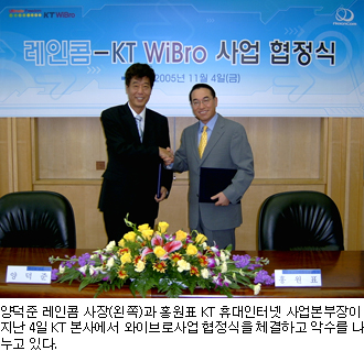
휴대형 멀티미디어 기기업체 레인콤(대표 양덕준)이 내년에 내놓을 휴대형 게임단말기가 KT의 휴대인터넷(와이브로)망을 통해 온라인 서비스된다.

레인콤은 KT와 이같은 내용에 대해 지난 4일 합의하고 협정식을 체결했다고 7일 발표했다.

레인콤은 KT의 와이브로망에 접속해 서비스받을 수 있는 특화된 단말기를 내년 8월에 출시할 예정이다.

레인콤은 원활한 서비스 제공을 위해 게임 전용 포털사이트와 플랫폼도 구축할 계획으로, 이 포털사이트는 레인콤의 와이브로 전용 단말기에 한해 동영상이나 음악, 메신저, 채팅 서비스를 제공하게 된다.

또 레인콤은 와이브로 단말기 출시를 기점으로 기존 단말기 분야에서 서비스분야로 사업영역을 확대해 무선 포털서비스 사업에도 진출할 예정이라고 밝혔다.

레인콤 미래전략연구소장인 신순철 상무는 "유무선 연동 서비스 등 콘텐츠를 원활하게 확보하기 위해 주요 게임 포털 서비스 업체와도 지속적인 교섭중"이라며 "단말기 완성도가 매우 높아질 것으로 기대한다"고 말했다.

양사는 와이브로 서비스 및 게임기 수요 확산을 위해 각사의 유통망을 최대한 활용해 가입자 유치 업무를 진행하는 등 적극적으로 공동마케팅을 펼치기로 했다.

Copyright(c) 2000. inews24.com All rights reserved.

2005년 10월 5일 수요일

Now, I'm in Singapore...^^;

엊그제 10월 3일부터 SINGAPORE 출장중이다... 다가오는 10월8일 한국으로 출발예정...

여기오면 무진장 더워서 고생할줄 알았는데, 생각보다 덥지는 않아서 다행~~~ 오히려 건물들은 너무 춥다...ㅋㅋ

Anyway, 이곳 특유의 딱딱 끊어지는 이상한 영어 발음들과 열심히 씨름중... (__") 뭐라카는지는 둘째치고, 일단 무슨 발음인지라도 정확히 알아 들었으면 좋겠당...^^;

놀러온것이 아니라 출장이긴 하지만, Stress 받을일은 없어서 그건 Good이다...헤헤헤

2005년 9월 15일 목요일

ECN Korea.com: 설계의 틀을 바꾸는 FPGA 설계 툴

본 메시지는 ECN Asia(Korea)에서 귀하께 발송한 것입니다:

Chang-woo YANG
cwyang@changwooyang.com

흥미로운 기사여서 전송합니다.

ECN Korea.com: 설계의 틀을 바꾸는 FPGA 설계 툴
http://www.ecnkoreamag.com/article.asp?id=1045

2005년 9월 7일 수요일

일상 생활에서 흔히 쓰이는 20가지 잘못된 영어표현

일상 생활에서 흔히 쓰이는 20가지 잘못된 영어표현

  1. 핸드폰 hand phone ---------------------------> cellular phone
  2. 자동차 핸들 handle ---------------------------> steering wheel / wheel
  3. 리모콘 remocon ------------------------------> remote controller / remote
  4. 매스컴 mass com ----------------------------> mass media / mass communication
  5. 모닝콜 morning call ---------------------------> wake-up call
  6. 아르바이트 arbeit -----------------------------> part-time job
  7. 아이쇼핑 eye shopping -----------------------> window shopping
  8. 호치키스 hotchikiss ---------------------------> stapler
  9. 에어컨 aircon --------------------------------> air-conditioner / air / AC
  10. 애프터서비스 A/S(after service) --------------> warrantee service
  11. 비닐봉투 vinyl bag --------------------------> plastic bag
  12. 탤런트 talent --------------------------------> actor / actress
  13. 와이샤쓰 Y-shirt ----------------------------> dress shirt / white shirt / shirt
  14. (남녀의) 미팅 meeting ----------------------> blind date
  15. 황금시간대 golden time ---------------------> prime time
  16. 휘발유 oil ----------------------------------> gas / gasoline
  17. 사이다 cider(사과주스) ---------------------> 7-Up / Sprite
  18. 공중전화 박스 telephone box ---------------> phone booth / telephone booth
  19. 팬티 panties ------------------------------> underwear (남녀의 속옷 모두를 통칭)
  20. 오디오 / 전축 audio -----------------------> stereo / audio system