2010년 4월 2일 금요일

Replacing RS-232 with 802.11n wireless

June 10, 2009

By N. Venkatesh, Redpine Signals

The Wired Setup
The monitoring and control of medical equipment and devices are often carried out from a separate controller or server. The server may be in the vicinity of the equipment or may be at a remote location. Traditionally, a common means of connecting the two is via an RS-232 serial interface. Consider a set of sensors controlled by a sensor unit as shown in Figure 1. The accumulated data is transferred to a monitor via a serial interface.


Figure 1: Sensor Unit and Interface to Monitor
(Click on image to enlarge)

The multichannel A/D converter is typically within the microcontroller unit. The periodically sampled data is encapsulated in a predetermined packet format and sent on to the Monitor via the UART interface of the microcontroller.
The applications running on the microcontroller and the monitor (or server) ensure the means to transfer the sensor data meaningfully. The device application encapsulates the data using a protocol negotiated with the receiver of the data (the server in this case). The obtained data would be de-capsulated on the corresponding peer before passing it to the application. Figure 2 illustrates this process.


Figure 2: Wired Connection
(Click on image to enlarge)

There are many methods of encapsulation - one example for encapsulation of IP data is SLIP (Serial Line Internet Protocol). SLIP is a packet framing protocol that defines a sequence of characters that frame IP packets on a serial line. It provides no physical addressing or error control, for which it depends on upper-layer protocols. SLIP simply sends the data and then sends a signal marking the end of the data.

The Basic Wireless Setup
The wired connection in Figure 1 can be replaced by a wireless one based on 802.11 WLAN by connecting the device and the server with a serial to Wi-Fi bridge. The serial to Wi-Fi bridge provides a means of transporting the device data either employing layer-3 protocols or directly bridging it to the corresponding Wi-Fi bridge at the server.


Figure 3: Wireless Connectivity in the Infrastructure Mode
(Click on image to enlarge)

There are many advantages to using 802.11 Wi-Fi connectivity in medical devices. Firstly, Wi-Fi is close to being ubiquitous, especially in medical establishments, and therefore no special provisions need be done at the infrastructure end. Secondly, the use of standard TCP/IP transport, as opposed to proprietary protocols, enables the monitors or servers to be present practically anywhere " within the premises on the LAN, or at any remote location via the internet. Thirdly, in comparison to alternatives like Zigbee or Bluetooth, WLAN provides longer range, higher throughput, and with the right implementation, better energy efficiency through the use of higher data rates translating to longer battery life.

The Wireless Transport Mechanism using TCP/IP
The serial to WiFi bridge frames an IP packet from the data obtained through the device and transmit to any other node in the network as shown in the figure 4.


Figure 4: Wireless Connection through a Wi-Fi Bridge
(Click on image to enlarge)

The serial to Wi-Fi bridge incorporates a built-in TCP/IP stack, thereby abstracting the application devices of the nature of network with which the data transmission/reception is done.
Transmission involves the following steps:

  1. The device encapsulates the data as mentioned in the above section.
  2. The serial to Wi-Fi bridge attached to the device decapsulates the obtained data.
  3. The decapsulated data is passed through the TCP/IP stack in the serial to WiFi bridge forming an IP packet.
  4. The IP packet, fragmented if necessary, is framed in WLAN MAC format and transmitted through the WLAN air interface.
The following are the actions performed by the serial to Wi-Fi bridge on the server side for reception of the packet.
  1. The WLAN interface receives and reassembles the IP packet.
  2. The received IP packet is passed through the TCP/IP stack, with its integrity verified.
  3. The payload in the IP packet is extracted.
  4. The application on the serial to Wi-Fi bridge encapsulates the data obtained before sending the data through the serial interface of the server.
  5. The server decapsulates the data obtained from the bridge.

Wireless Peer to Peer Transport
The serial to Wi-Fi bridge transfers a proprietary packet by using a delimiter to identify the encapsulated data obtained from the device. Figure 5 and 6 depict such transfers. This mode is potentially a proprietary one and the wireless connection used is mainly in an IBSS or ad-hoc mode.


Figure 5: Wireless Connectivity through the Ad-hoc Mode
(Click on image to enlarge)


Figure 6: Wireless Transport without TCP/IP
(Click on image to enlarge)

In this scheme, the following are the actions performed for the transmission:

  1. The device encapsulates the data as mentioned in the section 1.
  2. The serial to WiFi bridge receives the data from the device and adds the delimiter. This delimiter provides a way for the peer (bridge) to identify the encapsulated data.
  3. The data along with the delimiter is transmitted through the RF.
The following are the actions performed by the serial to WiFi bridge on the server side for the reception of the packet.
  1. The WLAN interface receives and assembles the packet.
  2. The received packet is processed to obtain the encapsulated data. The delimiter is used to identify the start of a data frame.
  3. The extracted data is sent through the serial interface of the server.
  4. The server decapsulates the data obtained from the bridge.
802.11n Benefits
Current serial to Wi-Fi solutions are largely based on 802.11b or 802.11g. Future enterprise networks are, however, likely to be predominantly 802.11n based, and recent serial to Wi-Fi products like Redpine's RS9110-N-11-22 are started catering to the 802.11n needs of the market. The IEEE 802.11n standard primarily provides for high throughput, high-efficiency, and long range data connectivity, and includes the use of multiple antennas and transmit-receive chains. However, the standard also includes a single-stream mode that is intended to provide the benefits of 11n to low-power small form-factor devices including sensor nodes. The use of single-stream 802.11n WLAN in these client devices provides the following benefits:
  • Higher throughput and lower transmit times " achieved through better efficiency in PHY and MAC.
  • Longer range " through use of multiple antennas at the access point
  • Preservation of 802.11n network capacity " the presence of legacy 802.11a/b/g clients forces the 11n nodes to use protection mechanisms and results in overall drop in network capacity. 802.11n helps avoid this.

Summary
802.11 WLAN, or Wi-Fi, is an ideal wireless transport mechanism for medical applications that currently employ the RS-232 serial interface for connectivity between sensors, devices, instruments, and monitoring equipment. Wi-Fi is ubiquitous as well as flexible " enabling a variety of connection methods including peer-to-peer and infrastructure modes spanning both the local network as well as the wide area network. In particular, the 802.11n WLAN standard would provide the benefits of range, throughput performance, and interoperability; and would remain an ideal solution for these applications through future network upgrades.

About the author
N.Venkatesh has more than 23 years of experience in communications engineering with expertise in wireless systems design, chip design, telecommunications and optical networking. He is responsible for leading the development of wireless systems at Redpine's development center. He can be reached at n.venkatesh@redpinesignals.com

====================

출처: http://www.rfdesignline.com/showArticle.jhtml?articleID=217800953

‘나만의 이동 경로를 인터넷 지도에 남기자!’ 큐비랩 포켓GPS S1

Posted 2010-02-19 10:52:52 / 김영훈 기자

라이더는 물론 등산, 여행객을 위한 신개념 레저용 GPS

최근 휴가철이 막바지에 이르면서 자동차로 장거리 여행을 떠나는 이들을 심심 찮게 찾아볼 수 있다. 이러한 장거리 여행을 위해서 필요한 장비가 바로 내비게이션이다. 하지만, 시중에 출시되고 있는 대부분의 내비게이션은 자동차용으로만 국한돼 있는 것이 사실이다.

그렇다면, 자전거나 도보시에도 네비게이션과 같은 기능을 활용할 만한 장비가 없을까? 최근 내비게이션에 탑재되는 핵심 부품 중 하나인 GPS를 활용한 모바일 기기가 속속 모습을 드러내고 있다.

GPS(Global Positioning System)는 전세계 어디서든 인공위성을 통해 자신이 위치한 장소를 파악할 수 있는 기술로서, 앞서 설명한 내비게이션은 물론 휴대폰에 이르기까지 다양한 모바일 기기에 탑재되고 있는 대표적인 위치 기반 시스템 중 하나다.

여기에, 최근에 출시된 아이폰이나 옴니아2와 같은 고성능 스마트폰에도 GPS가 탑재돼있어 언제 어디서나 자신이 위치를 파악할 수 있다는 장점을 가지고 있지만, 현존하는 대부분의 스마트폰은 전화와 GPS 기능을 동시 사용하기에 한계가 따르기 마련이다.


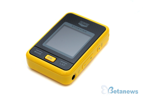
▲ 큐비랩 스토리쉬 포켓GPS(PocketGPS) S1

큐비랩이 출시한 ‘스토리쉬 포켓GPS S1’은 국내 기업으로는 처음으로 순수 개발된 제품으로서, 자전거를 활용한 운동 및 여행은 물론 도보, 등산시 자신의 위치를 인터넷을 통한 지도 서비스를 통해 기록할 수 있는 신개념 레저용 GPS 단말기다.

깜찍하면서도 심플한 디자인에 폭넓은 부가 기능 돋보여


▲ 컴팩트한 사이즈로 휴대성을 높이는 데 일조했다

스토리지 포켓GPS S1은 앞서도 설명했다시피 장시간 자전거를 타고 여행이나 운동을 즐기려는 라이더는 물론, 도보 및 등산시 자신이 위치하고 있는 장소를 구글 어스와 같은 인터넷 지도로 기록해 활용할 수 있는 제품이라고 할 수 있다.

여기에, 얼핏 보면 휴대용 GPS가 아닌 초소형 MP3가 연상될 정도로, 깜찍하면서도 심플한 스타일에 초점을 두고 있다는 것을 쉽게 확인할 수 있다. 또한, 각 모서리의 라운딩 처리와 함께 옐로우 컬러를 채택해 다소 딱딱한 느낌 보다는 산뜻한 분위기를 물씬 풍긴다.

그 뿐만이 아니다. 배터리 4개가 들어간 것과 별반 차이가 없을 정도로 상당히 컴팩트하고 슬림한 사이즈를 부각시켰으며, 무게 또한 휴대폰 보다도 훨씬 가벼운 60g에 불과하기 때문에 잦은 이동에도 뛰어난 휴대성을 보여줄 수 있도록 했다.

특히, 이번 제품은 밤낮을 가리지 않고 휴대하는 사용자를 고려해 OLED(자체발광형 유기물질) 디스플레이를 탑재해 퀄리티를 극대화시키는 데에도 일조하고 있다.

OLED는 일반적인 모바일 기기에 탑재되는 TFT-LCD와는 다르게 자체발광이 가능해 어떠한 환경에서도 밝은 화면을 보여준다는 장점을 가지고 있으며, 실제로 모 대기업의 제품에서 대표적으로 사용되는 디스플레이 방식 중 하나로 수많은 소비자들에게 각광받고 있다.


▲ 초보자도 쉽게 사용할 수 있도록 버튼 구성을 간소화시켰다

▲ 평균속도 및 해발 고도, 나침반 등의 총 5가지 모드를 탑재하고 있다

제품 하단부에는 GPS 및 다양한 부가 기능을 활용할 수 있는 모드(MODE) 버튼을 시작으로, 자신이 이동했던 거리를 단말기로 기록하기 위한 랩(LAP), OK 버튼 등 3가지로 간단하게 구성돼있기 때문에 제품 조작에 미숙한 초보자도 간편하게 사용할 수 있도록 배려했다.

그 중에서도 모드 버튼의 경우 총 5가지로 구성돼 있으며, 기본모드는 1초 간격으로 GPS 로그를 자동적으로 저장해 라이딩 및 도보를 통한 운동, 등산 등에서 활용 가능하며, 운동모드와 고도모드는 구간별 거리 및 시간은 물론 현재 평균속도, 해발 고도를 한눈으로 쉽게 알아볼 수 있다.

특히, 이번 제품에는 고가의 GPS 장비에서만 찾아볼 수 있는 기압 센서를 이용한 고도 측정이 가능하도록 설계돼있다. 이 기능은 제품이 켜진 상태의 위치를 기준으로 고도 그래프를 정밀하게 확인할 수 있다는 장점을 가지고 있어 등산을 즐기는 유저라면 필수적이다.

이밖에, 해당 위치에 대한 위도 및 경도값을 표시하기 위한 나침반 모드는 물론, 현재 수신 중인 위성 정보 및 수신 세기에 따른 위도, 경도를 파악하는 것 또한 가능하다.


▲ 단순 GPS 단말기임에도 불구하고 녹음 및 MP3 재생 등의 다양한 기능을 갖췄다

스토리지 포켓GPS S1은 단순히 제품명으로만 보더라도 GPS 수신기로 생각하는 사용자들이 적지 않을 것이다. 하지만, 이번 제품에는 GPS를 통한 위치 수신 및 이동 거리 측정은 물론, 녹음 및 MP3 플레이어에 이르기까지 다양한 기능을 탑재한 점이 가장 큰 특징이다.

녹음 기능을 활용하기 위해서는 전원이 켜진 상태에서 우측의 위치한 REC 버튼을 길게 3초이상 누르고 있으면 보이스 레코딩 화면으로 전환되면서 쉽게 녹음이 가능하며, 자신이 즐겨드는 MP3 음악을 제품 내부에 탑재된 플래시 메모리로 저장할 수 있다. 참고로 저장 공간은 1.6GB로서 100여개의 MP3 파일을 담아도 전혀 부족함을 느끼지 못한다.

다만, MP3 파일을 넣은 뒤에는 반드시 ‘LP20100228_230001.MP3’와 같이 파일 이름을 변경해야만 정상적으로 재생이 가능하며, 일반 파일명으로는 재생이 불가능하다는 점을 인지하고 있어야 한다. 여기에, 단순 재생만 가능하다는 점도 차후 펌웨어 업데이트를 통해 해결해야할 개선책임에는 틀림없다.


▲ 외장 하드디스크에서 널리 활용되는 미니 USB 인터페이스를 탑재

스토리지 포켓GPS S1의 좌측부에는 PC 연결을 ㎸?미니-USB 포트가 위치하고 있으며, 케이블 연결을 통한 충전이 가능하다. USB 케이블을 통해 완충까지 소요되는 시간은 4시간이며. 최대 휴대할 수 있는 사용시간은 밝기 설정에 따라 최대 11시간까지 가능하다는 것이 큐비랩 관계자의 설명이다.

여기에, 앞서도 설명했다시피 녹음된 파일을 PC로 전송하는 것은 물론 자신의 PC에 저장된 MP3 파일을 내장 메모리로 추가할 수도 있으며, 초보자를 배려한 PDF 규격의 사용 설명서와 함께 GPS 기능을 활용할 수 있는 프로그램이 내장돼있다. GPS 기능 활용에 대한 부분은 다음 페이지에서 알아보도록 하겠다.


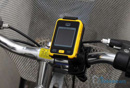
▲ 자전거에 활용하기 위해서는 별도의 자전거 거치대를 구매해야 한다

GPS 로그 기록을 위한 소프트웨어 제공은 기본!

▲ 로케이션 플러스 PC 툴에는 구글 어스가 기본으로 포함돼있다

스토리지 포켓GPS S1은 단순히 제품만으로 모든 기능을 사용하기에는 한계가 있다. GPS 수신을 통한 위치 정보를 지도로 한눈에 확인하는 것은 물론, 자신이 이동했던 장소가 정확하게 어디 지점인지를 파악하기 위한 소프트웨어도 뒷받침되어야 하기 때문이다.

이번 제품에는 이러한 사항을 간편하게 해결할 수 있도록 ‘로케이션 플러스 PC 툴(Location Plus PC Tool)’이라고 불리는 부가 소프트웨어를 기본으로 제공해 단말기 사용에 따른 편의성을 극대화시켰다.

특히, 이 프로그램에는 무료 지도용 소프트웨어로 전세계적으로 명성을 떨치고 있는 구글 어스(Google Earth)맵이 포함돼 있다. 구글 어스에는 포털 서비스 못지 않는 정확한 장소 확인은 물론, 위성을 활용한 스카이뷰, 심지어는 고도 확인까지 한눈에 파악 가능하다.

또한, GPS를 켜고 마지막으로 끈 상태까지의 모든 기록이 남기 때문에, 자신이 이동했던 장소를 별다른 어려움 없이 확인할 수 있다.

물론, GPS 자체가 전파 장비에 약하고 자동차나 특정 건물로 들어갈 경우에는 정상적인 인식이 되지 않는 경우도 발생할 수 있기 때문에, 제품을 손으로 직접 들고다니며 사용하는 것이 좋다. GPS 최초 수신시에는 평균 5초 이내로, 일반 GPS 단말기보다는 빠른 편이다.


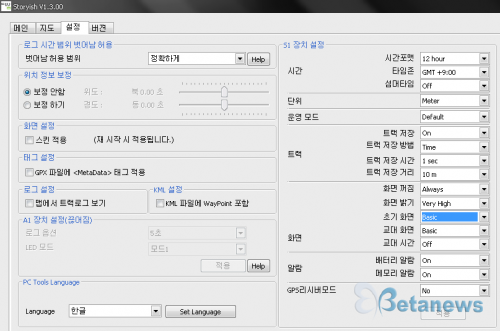
▲ 제품에 대한 장치 설정 및 위치 보정 등이 가능하다

로케이션 플러스 PC 툴의 설정 화면으로 진입하면 GPS 위치 보정은 물론 로그 및 화면, 언어 등이 세부 설정이 가능하며, 장치 설정의 경우 제품에 탑재된 OLED 디스플레이의 화면 밝기 설정과 시간, 트랙, 알람 설정에 이르기까지 다양한 부가 기능이 포함돼있다.

또한, GPS 리시버 기능을 활성화할 경우 별도의 내비게이션을 구입할 필요 없이, 자신의 PC에 설치된 내비게이션 프로그램으로 지도 안내 서비스를 활용할 수 있도록 선택의 폭을 넓힌 것도 이번 제품의 차별화된 장점이다.

◇ 휴대폰에 GPS 기능이 없다면? 큐비랩 스토리시 포켓GPS S1이 대안 = 최근 GPS 기능이 기본 탑재된 최신 휴대폰 및 스마트폰을 시작으로, 다양한 모바일 기기들이 속속 국내 시장에 모습을 드러내고 있다.

하지만, 대부분의 사용자들은 자신의 모바일 기기에 GPS 기능이 있는지 조차도 알 수 없고, 막상 기능이 포함돼있다고 하더라도 제대로 활용하지 않는 경우가 다반사다.

물론, GPS가 우리 생활에 큰 영향을 끼칠 만큼 중요하지 않을 수도 있으나, 여행이나 등산, 자전거를 통한 장거리 이동을 즐기는 유저들이라면 GPS만큼의 필수적인 장비는 찾아보기 힘들 것이다.

이번에 선보인 큐비랩 스토리시 포켓GPS S1은 일반적으로 휴대폰에 내장된 GPS 수신기와 동일하기는 하지만, 평균 속도와 해발고도, 위도 및 경도값을 표시하기 위한 나침반에 이르기까지 다양한 기능을 갖추고 있다는 점에서 상당히 매력적인 제품이라고 할 수 있다.

물론, MP3 플레이어 활용시 재생만 가능하고 GPS 수신시 일부 오류를 일으킨 점이 다소 아쉽기는 하지만, 홈페이지를 통한 지속적인 업데이트로 충분히 개선 가능한데다가 국내 기술로 만들어진 레저용 GPS 중에서는 최초라는 점에서 더욱 의미가 크다.

가격 또한 20만원이상의 턱없는 가격대를 유지하고 있는 일부 외산 제품에 비해, 큐비랩 스토리시 포켓 S1은 10만원대로 비교적 저렴한 데다가 성능 또한 고급형 제품 못지 않는 뛰어난 GPS 수신율를 보여준다는 장점만으로 최상의 메리트를 보여줄 것으로 기대된다.

/ 베타뉴스(http://www.betanews.net)

==========

출처: http://www.betanews.net/article/487965&ad=1058

2010년 3월 12일 금요일

TierLogic lifts the veil: another take on the 3D FPGA

Wednesday, March 10, 2010

TierLogic, yet another large and expensive FPGA start-up that has been in stealth mode for years, today unveiled a radical approach to increasing the density and utility of large programmable logic devices. Like previously-announced Tabula, TierLogic describes their design as a 3D FPGA. But the two approaches are totally unlike each other, and neither is related to the concept of 3D ICs—involving stacked dice and through-silicon vias—that is currently the hot topic in SoC-of-the-future circles.

TierLogic's big idea is elegant and audacious: increase the density of FPGAs by moving all the configuration memory—not the data memory or the look-up-table (LUT) memory, but the RAM cells that control the interconnect muxes—out of the silicon. Removing these memory bits by itself can cut die area—at least the die area occupied by logic fabric—more than in half, according to the company's vice president of sales and marketing, Paul Hollingworth. TierLogic employs this advantage to use a mature 90nm process node and still deliver a smaller die area than a conventional SRAM FPGA would require, making it possible to offer the FPGAs at about half the cost of equivalent conventional parts.

But those SRAM cells have to go somewhere. That's where TierLogic's foundry partner Toshiba comes into the picture. Toshiba has developed a unique back-end-of-line process that puts a layer of amorphous-silicon thin-film transistors (TFTs) on top of the interconnect stack. The proprietary process uses virtually none of the wafer's thermal budget, so it's compatible with advanced CMOS. Yet at 180nm dimensions Toshiba can produce sufficiently fast and dense TFT SRAM cells to accommodate all the configuration memory required for the FPGA below. And since the configuration SRAM just sits there providing steering bits to the muxes—no user delay paths pass through the configuration memory—the slower, more stable TFT SRAM has no impact on user timing, except for the significant benefit of allowing the active die area be much smaller.

So this is what TierLogic means by 3D: the chips have two separate layers of active circuitry. The substrate holds the logic cells, interconnect muxes, block memory, and other user-accessible features. The TFT layer on top of Metal-8 holds the configuration memory. The result is an FPGA that can be functionally equivalent to industry-standard devices, but potentially on smaller dice, and so significantly lower in cost and power. Hollingworth said that in practice, TierLogic parts will be about 30 percent denser than economy FPGAs and 2.6 times the logic density of high-end conventional devices. For reasons we'll discuss later, TierLogic is also claiming about a third better logic-cell utilization, so overall the company boasts over three times the logic density of existing high-end FPGAs.

There is a second major advantage to this two-layer implementation: ASIC conversion. Since the TFT SRAM cells are not in any user timing paths, TierLogic can replace the TFT layer with a simple metal layer containing hard straps to power and ground busses, and have no impact on user timing (except of course for eliminating the need for a power-up configuration mode.) Eliminating the TFT layer reduces cost further, creating a mask-programmed device that is functionally- and timing-equivalent to the field-programmable device, but cheaper. "This is the first time there has been an ASIC solution that really fits for volumes between a hundred and ten-thousand units," Hollingworth maintains.

The turn-around time for reducing a fuse map to a metal-mask and delivering the mask-programmed parts is four weeks. No redesign is necessary, nor should there be any need to reclose timing, although some customers will still have to requalify the parts. The quick turn-around is in part because TierLogic can bank all its wafers at Metal-8, and simply send the wafers to either the TFT line or to Metal-9 fabrication, as needed.

This capability gives TierLogic the equivalent of Altera's Hardcopy capability—with die size and cost intermediate between an FPGA and a cell-based ASIC—but without requiring the customer to redo timing closure with a new set of timing files. The company is underlining this point by offering to early adopters that TierLogic will do the conversion from an existing production or prototype FPGA design or ASIC design to a TierLogic metal-programmed part as a service. For a minimum order of 50k units the service is free. The company will give you complete pin-compatibility with your existing part for a small NRE, or throw pin-compatibility in as well on a 100k-unit minimum order.

The tool flow for the devices is familiar: Mentor Precision Synthesis followed by proprietary mapping, routing, and analysis. One interesting point in the mapping process is that TierLogic's LUTs are fracturable. If a path requires only a portion of a LUT—an inverter, say—the rest of the LUT is available to other nets. "Fracturing is known to be valuable—it improves our logic-cell utilization by 36 percent," Hollingworth said. "But if your configuration RAM is on your die, it's just too costly to support fracturing."

Apparently Tabula's announcement persuaded TierLogic to announce a little earlier than they had intended. The company is not ready to give detailed product descriptions yet. Hollingworth did say that the mask-programmed version of the parts is available today, so TierLogic invites interested prospects to register on their site and get more detailed information. The company has already done one design that includes an on-chip MIPS R4000 CPU implemented in the logic fabric, for example.

Hollingworth expects to ship engineering samples of the field-programmable part with the TFT SRAM layer by the end of June this year, but it will be a while longer before those devices are qualified for full production. There are still issues with TFT yield, he admitted, but the company has seen a new run that appears to solve the problem. It just has to be fully evaluated.

In the future, TierLogic has several options. Hollingworth said that the engineering team has done critical-dimension analysis that indicates the TFT approach will scale to at least the 40nm node, giving the idea lots of room for evolution. And there are at least two more revolutionary ideas afoot. First, since the TFTs are relatively low-performance devices processed at low temperature, the TFT layer is compatible with just about anybody's advanced CMOS process. So TierLogic can license a field-programmable logic fabric as IP for use inside a cell-based SoC. You could have your wafers built at your favorite foundry, passivated and shipped to Toshiba, who could strip the passivation and fabricate the TFT layer. Hollingworth said that the company has already had discussions along these lines with some prospects.

The second point Hollingworth mentioned is that Toshiba is looking at the laser-annealing process that is coming on-stream for the 32nm process node. Once the laser-annealing systems are developed and in place, the high-speed laser annealing could create the local high temperatures necessary to produce a much higher-performance TFT without impacting the thermal budget of the underlying wafer. This would in principle allow TierLogic to put not just configuration memory but signal-path devices such as embedded SRAM blocks and even some logic structures or analog circuits in the top layer, creating an even denser FPGA. But that is for the future.

© Reed Business Information, a division of Reed Elsevier Inc. All rights reserved.

=======

출처: http://www.edn.com/blog/1690000169/post/1870053187.html

Tier Logic's Threefold Path

Wednesday, March 10, 2010

Tier Logic has gotten the occasional mention in this blog as a startup specializing in 3D interconnect, but after the splash made by players such as Tabula, NuPGA, and Abound, one could almost be tempted to ask what the company would do for an encore. But on the eve of Tier Logic’s official “architectural announcement” of March 10, Tier’s vice president of sales and marketing Paul Hollingworth clued me in on the company’s threefold path to profitability, which frankly makes a lot more tactical sense than what I’ve heard from other startups of late.

The company relies on relatively traditional configuration logic in a nine-layer-metal base, but adds TFT-based configuration SRAM in a third dimension, which can be replaced by the ninth layer of metal as a ROM configuration layer when committing a design to production. Tier Logic deliberately chose Toshiba as a process partner for its low-temperature amorphous silicon process, well-characterized in the display industry, as a more straightforward and economic alternative to polycrystalline silicon.

While nothing sounds radical from an architectural standpoint,  that is part of the point of providing designers multiple paths to design production, which carries the fringe benefit of giving Tier Logic multiple paths to profitability. Tier Logic is working with a core of customers today to convert traditional designs to its all-CMOS TierASIC devices. Within the second quarter of this year, Tier Logic will convert some existing designs to the TierFPGA device using TFT SRAM as configuration – and some of those designs may later convert to TierASIC if volume warrants. (Typical NREs for the ASIC conversion step will be less than $50,000.) By year’s end, as designers become familiar with the Mobius design suite that Tier Logic provided to first customers in early 2010, the company will accept verified designs as first-pass TierFPGAs, converting to the metal-characterized TierASIC when and if those customers desire.

Hollingworth got to play the ASIC-conversion game when he headed up the HardCopy effort at Altera. He said he was a little concerned about the number of FPGA startups being launched just as a major recession began, but examined the Tier Logic business plan and decided it had the best chance of actually carving a slice of market share from existing FPGA market leaders.

When Tier Logic can capture a customer’s attention, Hollingworth feels confident the smaller size and lower power dissipation of a TierFPGA can win customers from the Big Two. The Mobius suite, which uses standard capture and simulation tools, the Mentor Precision Synthesis package, and unique P&R and timing analysis tools from Tier Logic, offers a common flow for FPGAs and ASICs. The problem, as always, is gaining the customer’s mindshare as a startup. But Tier Logic figures its hurdles at breaking into the FPGA mainstream are less daunting than many FPGA startups, and the company may be right about that.

© Reed Business Information, a division of Reed Elsevier Inc. All rights reserved.

==========

출처: http://www.edn.com/fpgagurus/blog/890000689/post/1850053185.html

2010년 3월 9일 화요일

Embedded FPGAs

December 29, 2008

Check here for the lastest How-To technical articles on Embedded FPGAs, PLDs and other configurable devices as compiled by our Embedded.com sister site.

By Bernard Cole

For your convenience, collected here the most recent How-To and Technical Insight articles on Embedded.com on field programmable gate arrays (FPGAs), programmable logic devices (PLDs), and other  reconfigurable devices and systems. We are constantly updating this list, so check back occasionally to see what's new:

2008

2007

2006

2005

For more information on designing with field programmable gate arrays, field programmable logic and other reconfigurable devices, go to the Programmable Logic DesignLine Web Site.

We will regularly be reporting on all aspects of this important trend on Embedded.com in the form of news, features, product stories, columns, commentary, in-depth technical and how-to articles.

We welcome your participation and would like to hear from you. If you are a developer, let us know what problems you are facing and the solutions you are considering. If you are a hardware or software vendor, we want to know what you have got in terms of building blocks and tools, how they work and how to use them.

We also want to know what kind of information you need and what kind of stories you need to read as well as the kind of stories and contributions you can write for the site.

Call me at 602-288-7257 or email me at bccole@acm.org

==========

출처: http://www.pldesignline.com/200001906

2010년 3월 8일 월요일

Tabula FPGAs: this one could be game-changing

Monday, March 1, 2010

Tabula, a heavily-funded FPGA start-up led by a who's-who of FPGA- and EDA-industry insiders, this morning unveiled a new FPGA architecture that challenges fundamental assumptions about RAM-configured logic devices. Tabula claims it will deliver FPGAs that in the same device can offer 1.6 GHz clock rates on critical paths, logic and memory capacity comparable to the largest new devices from Altera and Xilinx, rich SerDes, DSP, and memory resources, and yet a die size small enough to sell at a fraction of Stratix IV or Virtex 6 prices. And, despite the startling claims, the devices will use a familiar tool chain and will look to the user like traditional FPGAs.

Such claims clearly require and explanation. Tabula is not claiming a revolution in process technology—the design employs fairly normal 40nm CMOS—or in logic architecture—to the user the Tabula devices will appear as an entirely familiar array of look-up tables (LUTs), latches, and configurable interconnect. Rather, Tabula's main innovation is to exploit brilliantly a growing imbalance in conventional FPGA implementation.

That imbalance is the disparity between the die area required by interconnect and that required by the logic elements and switches. By the 40nm generation, FPGA logic fabric has become a dense network of interconnect wires covering a very sparse array of LUTs, latches, multiplexers, and buffers. There is space on the silicon for more logic cells, but there is no room to get interconnect to them. You could make the LUTs, which are essentially 1x8 or 1x16 SRAMs, much larger, but studies have shown that his would not improve logic density for real designs. So while the lower routing and via layers are crowded, the space on the surface of the silicon is increasingly underutilized.

Tabula isn't interested in giving a detailed description of what they've done—they much prefer conceptual metaphors—but here's the idea. Instead of putting a single set of interconnect muxes, a LUT, and a latch in each logic cell, Tabula puts in eight of everything. Then they time-domain multiplex those eight sets of hardware on a 1.6 GHz master clock, so that the physical logic cell has a whole new personality—new interconnect routing, new LUT, and new latch configuration—every 600ps. Over the course of 5ns, the physical logic cell is, in effect, eight different logic cells.

Now the rest of the secret sauce. Tabula embeds transparent latches in the interconnect where it passes through the physical cell, and controls these latches with the time-multiplexing circuitry as well. So on each clock cycle, Tabula captures the state of the interconnect and logic cell in the latches. This allows the chip to pass the output of the LUT, for instance, to the input of the same or a nearby physical LUT on the next clock cycle. All the state that goes in flight during an eight-cycle sequence is available to drive cells on subsequent cycles. It is almost as if the FPGA had eight times as many logic cells as it actually does.

Tabula illustrates this concept as a three-dimensional chip of eight layers. Each logic cell connects to nearby cells around it on one layer, and to nearby cells above it on the next layer, in an expanding cone. In practice, users can visualize their design spread across the three dimensions, or mapped onto a single flat FPGA. However you choose to visualize it, you submit a netlist with timing constraints, and the tools map your nets across physical logic cells and interconnect, and across clock phases, to meet your constraints. Critical nets get mapped vertically, where they can often stay within one physical cell with essentially zero flight time. Nets with more slack get spread more widely across the die.

The architecture has several important implications. first, it packs about three times more logic into a given area than a conventional FPGA. Second, Tabula can emulate eight-port embedded RAM blocks by time-multiplexing the inputs and outputs of a single-port physical RAM, so the company can implement memory that is physically faster, denser, and lower in both static and dynamic power than the true eight-port blocks on a conventional high-end FPGA.

So yes, the claims on speed, density, and cost are plausible. Power is a more complex question. The devices implement a fine-grained clock-gating algorithm based on user signal activity, according to Tabula president and CTO Steve Teig. And the greater density means that the average interconnect length 80 percent shorter than on a conventional FPGA at the same geometry. Both of these factors sharply reduce dynamic power. But at the same time, there is the circuitry that manages the time-domain multiplexing activity, spread across the die in stripes and running at that 1.6 GHz clock frequency. "The net power compared to a conventional FPGA is design-dependent," Teig says. "The architectural overhead may or may not swamp out the savings."

So there is the story: speed, density, low cost. Tabula is aiming initially at the network switch sockets that make up the sweet spot of the high-end FPGA market. Presumably, the company will offer the configurations, on-chip peripherals, and IP those applications require. Specific product announcements should be coming soon, Teig says.

© Reed Business Information, a division of Reed Elsevier Inc. All rights reserved.

==========
출처: http://www.edn.com/blog/1690000169/post/1770052977.html?nid=2435&rid=8803234

2010년 3월 4일 목요일

삼성전자, 자일링스 28나노 제품도 생산

기사입력 2010-02-23
삼성전자가 파운드리 사업 가속화에 나섰다.

삼성전자(대표 최지성)는 세계 최대 프로그래머블 반도체(FPGA)업체인 미국 자일링스와 28나노 공정 파운드리(반도체 수탁생산) 계약을 맺었다고 23일 밝혔다. 자일링스와의 이번 계약은 지난해 45나노에 이은 두 번째다.

현재 세계 파운드리 전문 반도체 기업에서 28nm 공정을 개발중인 기업은 TSMC, 글로벌 파운드리 2개사에 불과하며 올해 3분기부터 양산에 들어갈 것으로 알려졌다.

삼성전자는 자일링스의 고성능 FPGA 반도체를 28나노 HKMG(High-K Metal Gate) 공정으로 생산할 예정이다. HKMG 공정은 유전상수가 높은 신물질을 사용해 누설전류를 줄이고 동작속도를 향상시킬 수 있는 차세대 파운드리 기술이다. 28나노 HKMG 공정으로 제품을 제조하면 기존 45나노 공정 대비 소비전력을 50%까지 줄일 수 있고, 28나노 미세공정을 이용해 칩 집적도를 두 배 이상으로 향상시킬 수 있다고 삼성전자는 설명했다.

민정기 삼성전자 반도체사업부 상무는 "28나노 HKMG은 32나노 공정에 이은 두번째 HKMG 공정으로, 삼성전자는 현재 시스템LSI 전용 300㎜ 팹인 S라인에서 이 공정을 개발하고 있다"고 밝혔다. 삼성전자는 45나노 공정으로 자일링스의 '스파르탄(Spartan)-6 패밀리' 제품을 현재 양산 중이며 28나노 HKMG 공정 제품은 내년부터 생산을 시작할 예정이다. 삼성전자는 28나노 이후 차세대 공정도 개발 중이어서 조만간 경쟁사들을 앞지르겠다는 목표다.

삼성전자는 파운드리를 차세대 성장동력으로 육성하기 위해 올해 초 조직개편을 통해 파운드리 센터를 파운드리 사업팀으로 격상시킨 바 있다. 삼성전자는 조직 개편을 통해 개발부터 영업까지 하나의 조직에서 총괄, 시너지를 냄으로써 매년 2자리 수 이상의 성장율을 기록하겠다는 목표다. 시장조사기관인 IC인사이츠에 따르면 삼성전자는 지난해 파운드리 사업 매출이 전년대비 12% 줄어든 3억2500만달러로 파운드리 업계 9위에 올랐다.

윤건일기자 benyun@etnews.co.kr

==========
출처: http://www.etnews.co.kr/news/detail.html?id=201002230022

2010년 3월 3일 수요일

알테라, 세 가지 신기술 결합한 28nm FPGA 연내 출시

알테라가 28nm 공정기술로 제작한 FPGA를 올해 안에 선보일 계획이다. 새로운 FPGA 제품군은 맞춤화가 가능한 하드웨어 IP인 '임베디드 하드카피 블록'과 부분적으로 재구성이 가능한 FPGA 영역, 그리고 28Gbps 성능의 트랜시버들로 구성된다. 이로써 소비전력과 비용 절감에 대한 요구 사항과 더 높은 시스템 대역폭 요건을 모두 충족한다는 게 알테라의 구상이다. NE-Korea

글_한덕선 기자(dshan@nekorea.co.kr)

모바일 인터넷과 FTTH, LTE/와이맥스 등의 가입자 수가 꾸준히 증가하고 HD 비디오 등 대용량 멀티미디어 데이터 전송이 점점 더 늘어나면서 대역폭 증대의 필요성이 높아지고 있다. 문제는 이를 이전과 비슷한 수준의 비용 및 전력 요건에서 처리해야 한다는 점이다.

지금까지는 무어의 법칙이 어느 정도는 통용되어 공정 노드를 축소함으로써 이러한 요구 사항을 해결할 수 있었다. 하지만 앞으로는 무어의 법칙 하나만으로는 이 문제를 해결할 수 없을 것으로 보인다. 누설 전류 문제를 외면할 수 없을 뿐만 아니라 아날로그 블록은 공정 축소로 쉽게 해결되지 않기 때문이다.

임베디드 하드카피 블록
알테라는 28nm 노드의 앞선 공정기술과 세 가지 혁신 기술을 함께 결합하여 이러한 요구에 대응하고자 한다. 혁신 기술에는 임베디드 하드카피(HardCopy) 블록, 부분 재구성 기술, 28Gbps의 트랜시버가 포함된다.

임베디드 하드카피 블록은 알테라 고유의 하드카피 ASIC 기술을 활용하는 맞춤형 하드 IP 블록을 말한다. 예컨대 특정 애플리케이션에 특화된 기능이나 독자적인 맞춤형 IP를 사용자가 일일이 프로그래밍하지 않아도 되게끔 한 것인데, 이를 통해 사용자는 타임투마켓을 앞당기고 개발 비용과 소비전력을 줄일 수 있으며, 알테라로서는 특정 시장 영역에 대응하는 다양한 제품들을 보다 신속하게 공급할 수 있다는 이점을 갖게 된다.

28Gbps 트랜시버 탑재
내장되는 트랜시버의 성능도 28Gbps로 향상되어 I/O 대역폭을 크게 늘리게 된다. 28Gbps 성능은 이전 세대 제품인 알테라의 40nm 스트라틱스 GT FPGA의 11.3Gbps 트랜시버보다 2배 이상 향상된 것이다. 트랜시버 성능이 높아지면 외부 부품 수와 I/O 핀 수를 줄일 수 있을 뿐 아니라 소비전력과 비용도 절감할 수 있다.

알테라의 제품 및 기업 마케팅을 담당하는 빈스 후(Vince Hu) 부사장은 "일례로 과거에 10Gbps 트랜시버 80개를 사용해야 했던 시스템 설계를 향후에는 25Gbps 성능의 트랜시버 32개를 사용해서 구현할 수 있다"며, "이 경우, I/O 핀 수가 80개에서 32개로 줄어듦으로써 보드 면적과 인터커넥션 등도 줄어들게 되며, 그 결과 제작 비용은 25~32%, 소비전력은 60%가 각각 저감된다"고 밝혔다.

'부분 재구성' 기능 지원
정상적으로 동작하는 FPGA의 구동에 아무런 방해도 주지 않고 해당 FPGA에 새로운 기능을 포팅하거나 시스템 업그레이드를 할 수 있는 기능도 추가된다. 이른바 '부분 재구성(Partial Reconfiguration)'이라는 기능이다. 알테라의 28nm FPGA는 크게 세 가지 기능 블록으로 구성되는데, 맞춤형 하드 IP인 임베디드 하드카피 블록과 고속 트랜시버, 그리고 재구성이 가능한 FPGA 영역이 그것이다. 이 가운데 재구성이 가능한 FPGA 영역은 디바이스가 동작하는 중에도 부분적으로 재구성이 가능하다. 알테라의 쿼터스(Quartus) II 디자인 소프트웨어 내에 포함되어 있는 점증적 컴파일(Incremental Compile) 디자인 플로우를 이용하면 부분 재구성 작업을 매우 간단하게 처리할 수 있다. 부분 재구성 기능은 소비전력과 비용을 절감할 뿐 아니라 작동하지 않는 기능들을 FPGA 내에 넣을 필요가 없게 만들어 로직의 실효 밀도를 높이는 효과도 제공한다.

빈스 후 부사장은 "최첨단 28nm 공정기술과 세 가지 혁신 기술들은 알테라 FPGA들의 밀도와 I/O 성능을 극적으로 개선시키고 ASIC 및 ASSP에 대한 경쟁력 우위를 더욱 강화시킬 것"이라며, "알테라는 이러한 혁신 제품들을 올해 안에 선보일 것"이라고 밝혔다.

==========

출처: http://www.nekorea.co.kr/article_view.asp?seno=6094

[2/23, ARM] 고성능 디지털 신호 제어용 동급 최고 Cortex-M4 프로세서 출시

고성능 신호 처리와 업계 최고 MCU 기술의 강력한 결합으로 급속하게 성장하는 하이브리드 DSC 시장 공략

ARM (한국대표: 김영섭)은 오늘 첨단 MCU(마이크로컨트롤러) 애플리케이션을 위한 혁신적인 Cortex(코어텍스)™-M4 프로세서를 출시한다고 발표했다. Cortex-M4 프로세서는 업계 최고인 ARM® Cortex-M 프로세서 제품군의 장점을 유지하면서 동시에 디지털 신호 제어(DSC: Digital Signal Control) 애플리케이션에 고효율의 솔루션을 제공한다.

특히 새롭게 부상하고 있는 모터 제어, 자동차, 전력 관리, 임베디드 오디오 및 산업 자동화 시장용 플렉서블 솔루션(flexible solution)의 요구사항을 충족하기 위해 고효율 신호 처리 기능과 Cortex-M 프로세서 제품군의 특징인 초저전력, 저비용, 사용 편리성 등이 완벽하게 결합되었다.

Cortex-M4 프로세서는 단일 사이클 MAC(Multiply-Accumulate) 장치, 최적화된 SIMD(Single Instruction Multiple Data)장치, 포화 산술연산 명령어(Saturating arithmetic instructions) 그리고 옵션으로 단일정밀도(single precision) 부동소수점처리장치(FPU: Floating-Point Unit)를 내장하고 있다. 이러한 디지털 신호 제어 기능은 ARM Cortex-M 프로세서 제품군의 특징인 혁신적인 프로세서 기술의 바탕 위에 구축되었다. 주요 기능으로는 1.25DMIPS/MHz 를 지원하는 고성능 32-비트 코어, 최적의 코드 밀도를 실현하는 Thumb(썸)®-2 명령어, 뛰어난 인터럽트 처리를 위한 NVIC(Nested Vector Interrupt Controller) 등이 있다. 이외에도 프로세서 동작의 유연성 증대를 위해, MPU(Memory Protection Unit), 저비용 디버그/트레이스 및 통합 수면 상태(integrated sleep states) 등과 같은 기능도 포함되어 있다. 임베디드 개발자들은 최대 성능과 극도로 낮은 전력 풋프린트를 가진 강력한 최종 제품을 신속하게 개발 및 제공할 수 있게 될 것이다.

디지털 신호 처리(DSP) 기술 기반의 시장을 분석하는 최고의 시장조사기관인 포워드 컨셉(Forward Concepts) 회장인 윌 스트라우스(Will Strauss)는 “임베디드 시장에서 신호 처리에 대한 요구가 전용 프로세서에서 하이브리드 마이크로컨트롤러로 바뀌고 있다. 이러한 제품들은 최고 수준의 디지털 신호 제어 기능을 구현하면서 다른 처리 연산을 효율적으로 수행할 수 있는 유연성도 동시에 제공한다”면서 “최적의 디지털 신호 제어 처리에 필요한 모든 기능과 Cortex-M 제품군 프로세서의 검증된 저전력 성능이 결합된 Cortex-M4프로세서 출시로 ARM의 파트너사들은 이러한 변화 추세를 십분 활용하게 될 것”이라고 말했다. 

Cortex-M4 프로세서는 물리적 구현을 위한 가장 폭넓은 파운드리 및 기술 지원을 제공하는 ARM 피지컬 IP 포트폴리오의 지원을 받는다. 여기에는 초 저전력 구현을 목표로 하는 파트너를 위한 TSMC CE018FG(180ULL) 공정용 Cortex-M Low Power Optimization Package (저전력 최적화 패키지)도 포함된다.

고성능 MCU 급 장치를 목표로 하는 파트너들을 위해서는 ARM은 주요 파운드리 공정에 관한 피지컬 IP 솔루션도 제공한다. 차세대 MCU 장치에서 150MHz를 목표 주파수로 하는 경우에는 65nm 글로벌파운드리(GLOBALFOUNDRIES) 65LPe 공정용 ARM 피지컬 IP를 이용하면, 65K 이내의 게이트와 40µW/MHz 이하의 동적 전력 소모를 보이는 Cortex-M4 프로세서 표준 구현이 가능하다. FPU를 포함할 경우는 25K 개의 게이트만 추가하면 되며, 이를 통해 업계 최고의 면적 풋프린트 이내에서 가장 강력한 구현이 가능하다.

SIMD와 FPU용으로 확장된 업계 표준의 ARM 컴파일러를 포함한 Keil(카일)™ MDK-ARM (마이크로컨트롤러 개발 키트)를 통해 Cortex-M4 프로세서용 개발 툴 지원이 제공된다. MDK-ARM은 µVision®4와 완벽한 Cortex-M4 프로세서 명령 시뮬레이션과 함께 첨단 트레이스 기능을 통한 타겟 디버깅도 포함하고 있다.

또한, ARM 아키텍처를 기반으로 하는 제품과 관련하여 설계에서 제작까지 완전한 솔루션을 제공하기 위해 제휴한 기업들로 구성된 업계 최대 규모의 에코시스템인 ARM Connected Community(커넥티드 커뮤니티)™회원사의 개발 툴, 디버거, RTOS 등도 Cortex-M4 프로세서를 지원한다. (세부사항은 아래 참조).


CMSIS (Cortex Microcontroller Software Interface Standard)

Cortex-M4 프로세서는 Cortex-M 프로세서 시리즈를 위한 벤더에 비종속적인 하드웨어 추상 레이어(vendor-independent hardware abstraction layer)인 CMSIS(Cortex Microcontroller Software Interface Standard)에 의해 완벽히 지원된다. CMSIS는 주변장치와 실시간 운영 시스템(RTOS)용 프로세서에 일관되고 단순한 소프트웨어 인터페이스를 구현해준다.

ARM은 현재 CMSIS를 확대하여 Cortex-M4 프로세서 확장 명령어에 대한 C 컴파일러(Compiler)지원과 MCU사용자들을 위해 신호 처리 프로그램을 쉽게 만들어주는 최적화된 라이브러리를 포함하려고 한다. 이 라이브러리에는 디지털 필터 알고리즘과 수학, 삼각법, 제어 함수 등과 같은 일반 함수가 포함될 것이다. 디지털 필터 알고리즘은 필터 설계 유틸리티와 MatLab(매트랩) 및 LabVIEW(랩뷰) 와 같은 설계 툴 키트와 함께 사용하도록 되어 있다.

이외에도, ARM은 Cortex-M4 하드웨어 및 소프트웨어에 관한 일련의 교육 코스를 개발했다. 이 교육 코스는 프로세서 출시와 함께 제공되어 라이선스 업체들이 Cortex-M4프로세서를 자신의 설계에 효율적으로 통합하고 최소한의 위험과 가장 빠른 시장 출시시간으로 최대 시스템 성능을 구현할 수 있도록 지원 할 것이다.

NXP, ST마이크일렉트로닉스(STMicroelectronics), 텍사스 인스트루먼츠(Texas Instruments) 등을 포함해 5개 주요 MCU 반도체 회사들이 Cortex-M4프로세서의 라이선스를 취득했다.

NXP 반도체의 마이크로컨트롤러 제품 라인(Microcontroller Product Line) 본부장인 조프 리스(Geoff Lees)는 “본사의 ARM Cortex 포트폴리오에 ARM Cortex-M4프로세서가 추가됨으로써 본사의 Cortex-M3 와 Cortex-M0 프로세서 기반 장치를 보완하게 되었으며, MCU 커뮤니티에 엔드-투-엔드 솔루션을 제공할 수 있게 되었다”고 말하면서 “Cortex-M4 프로세서는 이제 새로운 수준의 마이크로컨트롤러를 구현하여 신호 처리 시장의 고성능, 저전력 요구를 충족한다”고 덧붙였다.

ST의 마이크로컨트롤러 사업부문의 32-비트 마케팅 매니저인 세미르 하다드(Semir Haddad)는 “Cortex-M4 프로세서 도입으로 집약적인 수학 연산을 요구하는 애플리케이션까지 Cortex-M코어 사용을 확대 할 수 있게 되었다”면서 “Cortex-M4 프로세서 기반의 제품 라인이 본사 STM32마이크로컨트롤러 라인을 보완하여 본사 고객들은 STM32 확장성과 고급 신호 처리 기능을 결합할 수 있게 되었다”고 말했다.

텍사스 인스트루먼츠의 전세계 스텔라리스(Stellaris®) MCU 마케팅 총괄인 쟝 앤 부스(Jean Anne Booth)는 “Cortex-M4 프로세서는 PID 루프를 생성하며 상위 레벨의 모션 컨트롤을 향상시키고 더욱 신뢰할 수 있게 해줄 뿐 아니라 개발자들이 효율적인 모터 제어로 매우 높은 에너지 절감을 실현할 수 있게 한다”며, “또한 랩뷰나 매트랩/시뮬링크와 같은 메타 랭귀지 툴을 사용하는 비-프로그래머(non-programmer) 들도 ARM MCU 사용에 제한이 없게 되었다. 추가로, 내추럴/네이티브 C와 C++ 애플리케이션도 사용가능하여, 워크스테이션/전화/일반 임베디드 프로세서와 딥 임베디드 시스템에서 동일한 알고리듬을 사용함으로써 개발 시간과 위험을 줄일 수 있다”고 덧붙였다.

ARM의 프로세서 사업 부문 마케팅 부사장인 에릭 숀(Eric Schorn)은 “ARM이 본사 프로세서 제품에 DSP 기능을 포함시키기 시작한지 어느 정도 시간이 지났으며, 애플리케이션 시장에서 굉장한 성공을 거두어 왔다. 그러나 딥 임베디드 장치용으로 디지털 신호 제어 기능을 갖춘 프로세서를 설계 한 것은 이번이 처음”이라면서 “Cortex-M4 프로세서는 모터 컨트롤, 의료 기기, 자동차에서 산업 자동화, 전력 관리, 오디오 애플리케이션에 이르기까지 점점 늘어나는 임베디드 애플리케이션의 늘어나는 신호 처리 요구를 충족하기 위해 설계되었다”고 밝혔다.

==========

출처: http://www.semiconnet.co.kr/news_read.asp?seno=6828

2010년 2월 14일 일요일

Partitioning an ASIC Design into Multiple FPGAs

CMP - United Business MediaProgrammable Logic DesignLine

February 10, 2010

By Juergen Jaeger, Synopys Inc.

Most of today's system-on-chip (SoC) designs rely on field-programmable gate arrays (FPGAs) as a way to accelerate verification, start software development early and validate the whole system before committing to silicon. The FPGA may be an intermediate or, because tough economic realities cannot justify $1M+ in non-recurring engineering charges for an ASIC, initial implementation platform for the SoC design.

Today's FPGAs are large enough to contain a complex system-level design. It's practical, however, for these designs to be partitioned among several FPGAs for various reasons. For example, you may invariably need external components in your system. Also, using several smaller devices can enable a more cost-effective solution than using one big FPGA.

But, integrating your design into several FPGAs can create interesting partitioning problems, especially for larger and/or highly connected designs.

What are the Major Partitioning Considerations?

The most obvious problem for any design is the answer to the question: Will it fit into your FPGA prototype? If you have a very small design, you may fit everything onto a single, large FPGA and you technically won't have a real partitioning problem.

Figure 1: ASIC design start sizes

A note of caution: even though you may think that your design fits based on the ASIC gate count, your design may still need to be partitioned because of the resources available on the target FPGA. Memory or DSP-intensive ASICs frequently fall into this category of design.

Based on the current design sizes as shown in Figure 1, one-third to one-half of ASIC designs will fit into one of today's large FPGAs. Assuming that you have a bigger design and partitioning is required, you need to carefully estimate the number of FPGAs required in your prototyping hardware.

When you must partition, the three big concerns to keep in mind are:

  1. Which blocks need to fit into which FPGA so that you do not exceed the capacity or other resources of the FPGAs in your hardware-prototyping system?
  2. How do you interconnect the FPGAs? Most ASIC designs will exceed the number of available I/Os in the FPGA. Pin availability is further compounded by trying to meet timing.
  3. Finally, ASIC designs often include elements that need to be converted to an appropriate form for an FPGA implementation, such as ASIC memories or gated-clock tree structures.

Compounding these concerns is the decision of whether you want to partition the design at RTL or later in the design phase, such as at the gate level. Both approaches have advantages and disadvantages and are also, in part, dependent on the rest of your design flow.

Partitioning at What Level?

One of the first questions to ask when you partition is whether you want to partition at a netlist-level abstraction or a higher level of abstraction. There are advantages and disadvantages to both. The primary advantage of partitioning at the netlist level is that the area estimations are easier to calculate and more accurate since your design is largely implemented with the optimizations already taken into account. So, it is easier to accurately estimate the gate count and know how much room you will need. Conversely, dealing with a very large database may make partitioning difficult to perform. For example, a design with 90,000 lines of RTL may have a file size of 3.5 Mbytes, while the same design in netlist format may be 6.4 Mbytes in size. The difference could be significantly greater if there is a significant amount of instantiated blocks in the RTL; a 4x difference would not be unusual. In addition, for debugging purposes, it is very difficult to discern from the large, flat netlist database what the problems are in the original RTL. Many things will have changed as the design went from an RTL implementation to a netlist implementation, including netlist names.

Manual Partitioning

Historically, many designs were partitioned manually. There are two major reasons for this. First, it may simply be standard procedure, the way things were always done. This is often the case when the new design has only minor changes from the old design, and partitioning may not be that difficult. The second reason for manual partitioning may be a lack of budget or time to invest in adding a new tool to a flow that already works. It is not uncommon to see designs partitioned in Microsoft Excel' with mapping to see the pin and trace assignments.

If you decide to partition manually, keep these factors in mind:

  1. You need to perform a chip floor plan to ensure that the partitions revolve around the design's bus structures and data paths. In other words, you need to make sure that timing-critical modules are kept together and in close proximity.
  2. You need to ensure that extra logic does not need to be placed next to multiplex signals when there are not enough I/Os between FPGAs. You also must have intimate knowledge of the FPGAs that you will be using to ensure that the correct resources are available for your partition to function as expected.
  3. Finally, you need to perform gated-clock conversions, such as the conversion shown in Figure 2, to ensure that your ASIC design uses the primary FPGA clocks without introducing skews or timing issues.

Figure 2: Gated clock conversion

For the most minor of changes to an existing design, the completely manual approach may be feasible, especially if done by an expert designer at the RTL level. But, for anything more complex, the manual option is not really "manual". Manual gated-clock conversion for a multi-million gate ASIC is impractical and is usually done through a script or user-written program. Similarly, the logic to multiplex signals between the FPGAs is also done through a user-written program. It would be very difficult to keep all the variables in mind without also writing error-checking routines to ensure that you have used the proper number of resources on the FPGA. It is also doubtful that floor planning can be done manually at the netlist level because of the database sizes and the fact that the design is already near a final implementation phase.

Remember, too, that the cost of using the manual partitioning approach is not just the cost of doing things manually, but also the cost of writing and maintaining the conversion and checking programs that need to be written to make the partitioning of a large ASIC feasible. For large designs, except for companies with large internal CAD teams, it is quite likely that the cost in terms of time and support will be prohibitive.

Automatic Partitioning

A small number of vendors offer automatic partitioners. Any automatic partitioning tool should offer the following features:

  1. The ability to consider and optimize for both area and pin requirements to reach a viable solution.
  2. The ability to run at both an RTL and a netlist level of abstraction (An existing design requiring minor changes might be done at the netlist level, while a new design might be at the RTL level.)
  3. Quick area-estimation capability to give you a general feel and confidence that your design will fit onto your prototyping board.
  4. Understanding of the functionality and capabilities of your prototyping board. For example, if your prototyping board has dedicated high-speed clock lines, the partitioning tool's ability to recognize and utilize this functionality greatly enhances your ability to meet system timing.
  5. The ability to set threshold levels to control the amount of logic allocated to each FPGA. You want to be able to set the lowest threshold possible because a near-capacity FPGA may lead to long place and route times. Conversely, you may want to set a high threshold if you have a very large design and have a limited number of FPGAs on your prototyping board.
  6. The ability to have your automatic partitioning tool run on a board design with undefined traces. This allows you to determine if it is feasible to fit a design within the intended pin and area constraints before investing in the purchase or development of a board. Running on a board design with predefined traces produces a comprehensive signal-to-trace assignment report for detailed analysis.

Even with the features described above, it is unlikely that you will be able to fully automate the partitioning of a design without some prior knowledge or intervention. There are two major stumbling blocks to automation that most current tools do not address: (a) the ability to handle black box IP and (b) the ability to optimally utilize all the features within the FPGA such as block RAMs and DSP blocks.

The most efficient route to partitioning is to have a partitioning tool that has both manual and automatic features, such as the one shown in figure 3. Using this interactive flow, you can partition some sections of the design automatically while partitioning other sections manually, especially if you have design-specific information in mind.

Figure 3: Interactive partitioning

Integration Considerations

Up to this point, partitioning has been presented as an individual task in the verification flow. To successfully verify a design, a partitioning tool needs to easily fit into your team's existing flow. While a GUI is important, it is important that your tool be able to support TCL commands and create scripts as many ASIC designers script most of their designs. Support for standards like Synopsys Design Constraints (SDC) is also important. SDC support allows you to use your existing ASIC constraints to drive the partitioning process and ensures that your prototype system complies with other design requirements.

Debugging is a necessary step in ASIC verification. Your partitioning tool must be able to define probe points to allow internal signals to be monitored as part of the I/O interface. Integration with the most common FPGA debugging tools such as Xilinx's Chipscope, Altera's SignalTap and Synopsys' Identify greatly help the debugging effort and allow users to use the tools they are most familiar with. <.p>

Another key capability of a partitioning tool is that it supports the FPGA devices on the prototyping board. This may seem obvious but is often overlooked. While most commercially available partitioning tools support the largest Altera and Xilinx FPGA devices, some partitioners may not support legacy FPGAs or devices from other vendors. This additional FPGA device support gives you greater flexibility to build or buy FPGA hardware prototyping systems from vendors offering the best functionality or price for your needs.

Sound Partitioning Decisions

There are many ways to partition a design to fit into your FPGA prototyping hardware, and partitioning can be done at various phases and at different levels in the design process. With the exception of the most basic designs, a tool that offers both manual and automatic partitioning functionality can play an important role in your overall success. Equally important, this tool must be able to integrate into the overall design flow.

Yes, partitioning a large ASIC design into multiple FPGAs can be challenging. Doing some upfront planning and selecting the right tool flow can make it a lot easier, assure success and achieve the desired result: a thoroughly verified ASIC and first-silicon success.

All materials on this site Copyright © 2010 TechInsights, a Division of United Business Media LLC All rights reserved.

==========

출처: http://www.pldesignline.com/222700643

Digital camera differentiates itself by adding a second display

Performing a Tear Down on the Samsung TL225 digital camera revealed how they kept the BOM under control while expanding on the features.

By Richard Nass

Embedded.com (12/10/09, 09:47:00 AM EST)

It must be difficult for digital still camera vendors to differentiate their products from those of competitors, at least in the eyes of consumers. They can compete on resolution, battery life, image quality, etc. But those features are hard for the consumer to visualize, at least while in the store making a purchase. When you can come up with something that's truly different, then you have something you can really sink your marketing teeth into.

That's what the designers at Samsung have come up with—a digital still camera with a truly differentiating feature. The TL225, which happens to be the object of my current Tear Down, is built with a secondary display. It has the usual 3.5-in. display on the back. But the key is that it has a secondary display, measuring 1.5-in., on the front side of the camera.

The Samsung TL225 digital camera offers a differentiating feature—a secondary display on the front side of the camera.

If you're a 40-something like me, you may question why there's a display on the front of the camera. But show that camera to one of your kids like I did, and they know exactly what it's for—to take a picture of yourself or you and your buddies together.

The key for Samsung was to not raise the BOM much beyond what's required for a single-display camera. And they seem to have achieved that. Taking the camera apart showed that there are two key ICs on the board in addition to the memory.

Samsung was able to keep the BOM to a minimum by keeping the number of components to a minimum.

The Coach 10 device, from Zoran, drives the main display and also handles all the data conversion for the secondary display. In essence, the IC is connected to the image sensor on one side and the LCD on the other side. In between is the interface to the flash memory. The part corrects for image stabilization, lighting, and barrel effect, both in still mode and high-definition video mode.

Zoran claims to offer more than just the silicon. They provide many of the necessary algorithms, and even a reference platform that's pretty close to everything an OEM needs to go to market with a finished product. The Coach 10 also appears in Cisco's Flip UltraHD digital camcorder, which we took apart a few months ago.Note that Zoran has since released the next two devices in the Coach family, the 11 and 12. Those parts add features like face tracking, blur correction, noise reduction, and real-time lens distortion compensation.

The second part on the board is an Igloo AGL060 device from Actel, measuring 6 mm on a side. It's a flash-based FPGA that consumes very little power, operating down to 1.2 V. This particular part contains 60,000 gates and 96 user I/Os.

The Igloo FPGA is responsible for two key functions. One is to manage the interface between the Zoran part and the memory. And the second is to handle the interface to the secondary display. Hence, it's responsible for the LCD timing control and video downscaling.

The Igloo probably could have reduced some of the processing burden in the Zoran processor, had the Samsung designers chosen to do that. While that may have allowed for a slightly less powerful main processor, it would have required a lager die for the FPGA. That's an architectural decision the system engineer has to make. But the guess here is that they likely could have reduced both the bill-of-materials (BOM) and the power consumption slightly.

One of the nice features of the Igloo is that it can operate as either the master or the slave for power control. With a feature called Flash Freeze, the device goes into a very low power mode, around 10 μW. In this state, even though there's no logic toggling, I/Os can still be receiving data. But there's no power being consumed at the I/O or core level. Because the FPGA is flash-based, the value of the registers (or the memory itself) is not lost. Externally, there's no need to switch off the power, or gate or turn off the clock.

The software development for the camera was a designed mostly by Samsung, with drivers coming from Zoran and Actel. That makes the integration and validation a little tricky, because at the end of the day, or the end of the design in this case, all the pieces have to fit together, especially in terms of the timing and I/O assignments. Hence, there's a lot of finger crossing when you get to the validation stage. But in the case of the TL225, it's obvious that they got everything worked out, as the camera shipped on schedule.

On such a system, overall system validation could be difficult, in terms of developing pieces of code, making sure the timing and I/O assignments are accurate. You also have to make sure the footprint is right in terms of having everything fit properly on the board. I know that sounds obvious, but it should not be taken for granted.

Keeping the footprint as small as possible was key to the design.

The system's designers tell me that it worked right the first time, with just a little tweaking required on both the hardware and the software. This was likely because each subsystem was tested individually along the way. That increases the probability of things working correctly when they're all assembled together.

The design time for the TL225 was roughly five months from concept to completion. That's typical for a project like this one. While some of the pieces were new to this design, some IP was borrowed from previous designs, thereby fast-tracking the project somewhat.

==========

출처: http://www.embedded.com/underthehood/222001462

2010년 2월 1일 월요일

맥에서 윈도우 쓰는 제일 쉬운 방법

SCI-FOCUS

[ 제 904 호 ] 2009-04-20

정보통 씨는 예쁘고 세련된 디자인의 애플 컴퓨터에 자꾸만 눈길이 갔다. '기왕 쓰는 컴퓨터, 저렇게 세련된 제품을 쓰면 좋겠지'하는 생각에서다. 그러나 선뜻 애플 노트북을 살 수 없는 이유가 있었다. 정보통 씨가 다니는 회사의 인트라시스템에 접속하거나, 기존의 인터넷 뱅킹을 사용하기 위해서는 윈도우즈 PC를 써야만 하기 때문이다. 회사일을 집에서 처리하거나 은행 업무를 보기 위해서는 계속 윈도우즈 PC를 쓸 수밖에 없는 상황이었다.

그런데 얼마 전 정보통 씨는 그동안 눈독 들이던 애플의 노트북을 덜컥 사들였다. 최근 정보통 씨는 가상화 소프트웨어 덕분에 애플의 OS X(오에스 텐)에서도 윈도우즈 응용프로그램을 돌릴 수 있다는 사실을 알았던 것이다.

가상화(virtualization)는 컴퓨터에서 컴퓨터 리소스의 추출을 일컫는 광범위한 용어이다. 인터넷 백과사전인 위키피디아(wikipedia)는 가상화를 "물리적인 컴퓨터 리소스의 특징을 다른 시스템, 응용 프로그램, 최종 사용자들이 리소스와 상호 작용하는 방식으로부터 감추는 기술"로 정의하고 있다. 즉, 여러 가지 리소스(서버, 운영체제, 응용 프로그램, 저장장치)를 하나의 리소스처럼 보이게 하거나, 단일 리소스에서 여러 가지 물리적 리소스를 만들어 내는 것을 말한다.

좀 알쏭달쏭하게 들리지만, 실제 가상화의 구현 방식은 간단하다. 정보통 씨가 한 것처럼 한 대의 PC에 여러 가지 운영체제를 복수로 설치하여 동시에 사용하는 것, 이것이 가상화 기술이다. 다른 말로는 '플랫폼 가상화'라고도 불린다.

가상화 기술은 이미 1970년대 메인프레임 시절부터 사용되어 왔다. 에뮬레이션도 가상화의 한 예다. 최근 인텔이나 AMD의 x86 계열 CPU에서 가상화가 본격적으로 지원되면서 가상화 기술은 더욱 붐을 일으키고 있다. 플랫폼 가상화의 개념은 데이터 저장장치나 네트워크 리소스와 같은 특정한 시스템 리소스의 가상화로 확장되었다.

이제 정보통 씨는 사진을 정리하거나, 음악을 들을 때, 또 영화를 볼 때는 애플 노트북에서 기존의 OS X를 사용하다가, 사내 인트라에 접속하거나 인터넷 뱅킹이 필요할 때면 가상화 소프트웨어를 통해 MS 윈도우즈 창을 열어서 사용한다. 리눅스용 프로그램을 사용할 때면, 리눅스도 문제없이 띄울 수 있다. 정보통 씨의 애플 노트북은 한 대의 컴퓨터이지만 마치 여러 대의 PC를 사용하는 것처럼 쓸 수 있게 된 것이다.

가상화는 컴퓨팅 환경에 큰 변화를 일으키고 있다. 미국의 경제전문지 비즈니스위크나 포레스터리서치, 가트너그룹 등은 수년 전부터 가상화를 PC 분야의 가장 중요한 기술로 전망하고 있었다. 실제로도 가상화를 구현하는 소프트웨어 시장은 매년 60% 이상 성장해오고 있다. 가상화가 이처럼 빠르게 퍼지고 있는 것은 비용절감 효과가 크기 때문이다. 특히, 전 세계적인 경기불황으로 모든 기업이 경비절감에 힘쓰고 있는 상황에서 가상화는 더더욱 주목받을 수밖에 없다.

오늘날 기업 업무에서 IT 시스템은 필수적인 장비로 자리 잡았다. 결재는 물론, 기안, 사내 정보교류, 구매 및 입찰, 자산 관리, 재정, 웹 관리 등 대부분의 업무가 IT 시스템을 통해 이루어진다. 결과적으로 대부분의 기업은 전체 직원 수보다 더 많은 업무용 PC와 노트북 컴퓨터를 사용하고 있다. 이들 컴퓨터의 유지관리에 적잖은 비용이 들어가는 건 말할 나위도 없다. 그중에서도 각종 운영체제의 보안패치, 소프트웨어의 업그레이드, 각종 바이러스 및 보안 프로그램의 관리 등에 특히 큰 비용과 인력이 필요하다. 그 때문에 사내 업무용 PC를 효율적으로 관리하기 위해 가상화 기술을 도입하는 회사들이 늘고 있는 것이다.

최근 들어 주목받고 있는 '클라이언트 가상화 컴퓨팅'도 가상화의 일종이다. '클라이언트'는 중앙 서버에 연결해서 사용하는 개개인의 다양한 IT 기기를 뜻한다. PC, 노트북, PDA는 물론이고 아이팟, 휴대전화도 클라이언트가 될 수 있다. 이처럼 기기를 추가로 구입하지 않고 가상화를 통해 기존의 유휴자원 활용도를 높이는 기술이 클라이언트 가상화 기술이다. 기존의 장비를 그대로 활용하기 때문에 비용을 아낄 수 있고, 데이터센터에서 컴퓨터를 개별적으로 관리할 수 있어서 업무 효율성도 높일 수 있다.

이러한 가상화 기술을 도입하면 여러 이점이 있다. 직원들의 책상 위에 있는 PC를 얇은 클라이언트로 교체하게 되면 사무공간이 절약된다. 데이터센터에 위치한 서버 또는 얇은 블레이드 PC가 직원들의 PC를 대신하는 형태이기 때문에 전체적인 시스템의 관리가 한 곳에서 모두 이루어지고 장비 구입 및 설치 비용도 절약된다. 직원들은 인터넷이 연결된 곳이면 어디서든지 자신의 데이터에 접속할 수 있어서 업무효율성이 높아지고, 기업 입장에서는 바이러스 등에 대처하거나 기밀문서 유출 방지 등 각종 관리업무를 쉽게 할 수 있다.

그렇다면 우리 회사는 가상화를 통해 비용을 얼마나 아낄 수 있을까? 가상화에 대한 관심이 커지면서 가상화 도입을 통해 절약될 비용(장비 도입비용, 전기요금, 장소임대비용, 관리비용 등)을 계산해주는 사이트가 등장했다. 이러한 사이트에서 계산해보면, 가상화를 통해 전체 IT 장비의 유지보수 비용이 최대 50%까지 절감되기도 한다.

가상화를 통해 한 대의 컴퓨터에 하나의 운영체제만 설치되는 기존의 비효율적 환경은 크게 개선될 것으로 보인다. 또, 가상화 기술 덕분에 앞으로는 특정 운영체제가 시장을 독점하는 일이 드물어질 것이다. 정보통 씨의 사례처럼 MS 윈도우즈만 사용하던 사람들이 다른 운영체제를 동시에 사용할 수 있게 되었기 때문이다. 가상화는 회사의 비용을 절감해주고 개개인의 컴퓨터 사용을 편리하게 할 뿐만 아니라, 시장 질서까지도 바르게 재편해주는 '효자' 기술인 셈이다.

글 : 이식 박사(한국과학기술정보연구원 책임연구원)

Copyright(c)2006 KISTI All right reserved. 모든 저작권은 한국과학기술정보연구원에 있습니다.

==========
출처: http://scent.ndsl.kr/View.do?seq=4115&meid=1_2&class=100&gotoPage=4 &ordering=ISSUE&type=1&menu_id=104034&SearchText=&SearchGubun=SCENT&SearchYear1=2003 &SearchYear2=2010&onlyBody=FALSE